Wire Bonding

Advafab offers guaranteed high-quality mounting and wire bonding of its products together with its trusted partner.

image-1189

Die mounting and wire bonding services

AdvaFab offers mounting and wire bonding services for diode, 1D sensor and pixel sensor module products using its trusted production partners.

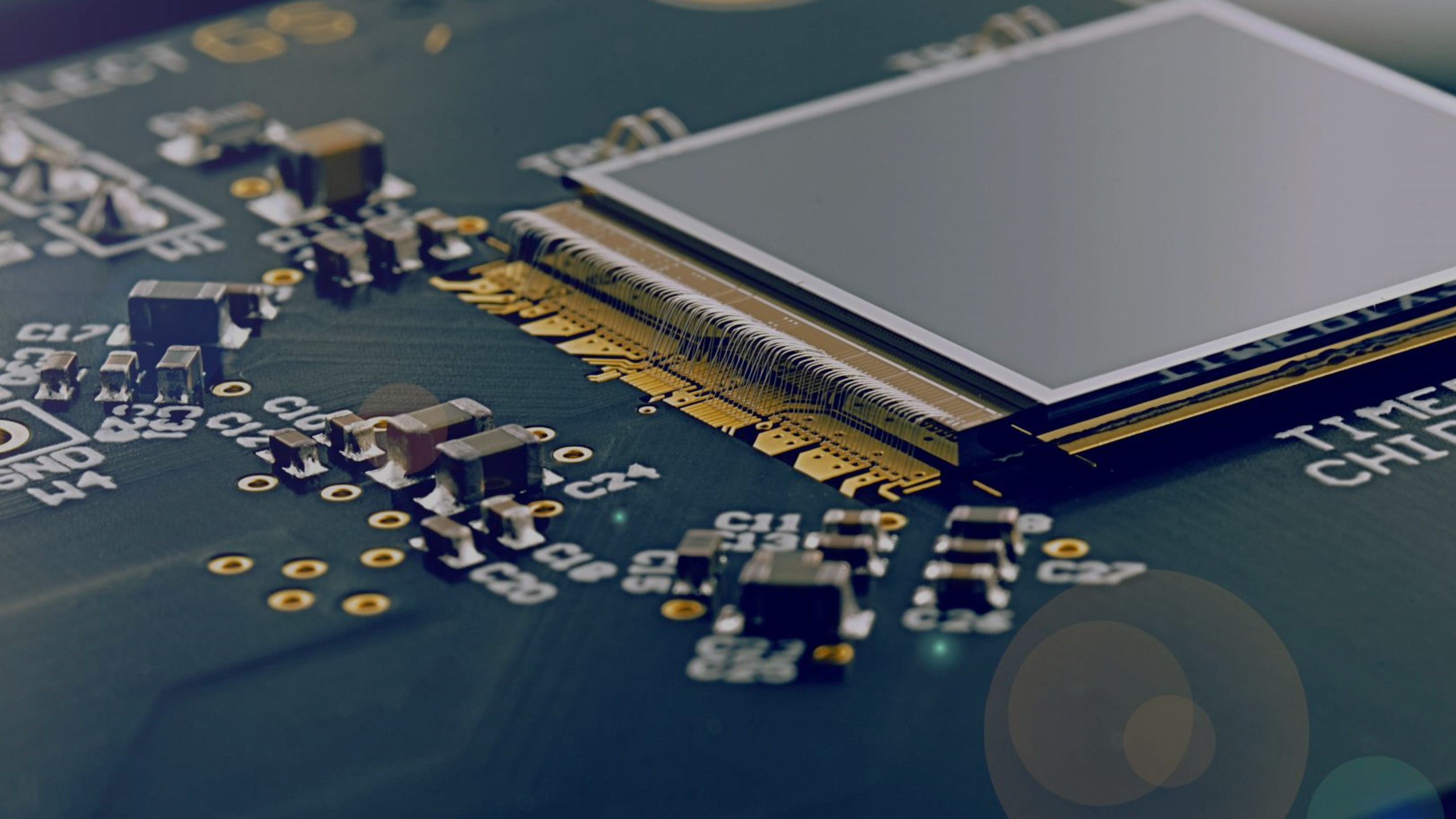
Component mounting on a PCB or ceramic, Al wedge and Au wire bonding services are offered for small batches or for large productions. In addition, manufacturing of the PCBs can be outsourced to Advafab’s partners.

image-1242

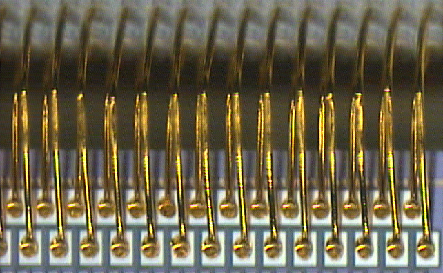
Wire bonding of 1D sensors.

  • The Si pixel sensors modules, diodes and 1D sensors can be mounted, cured and wire bonded at relatively high temperatures up to 250 C. Both aluminum and gold wedge wire bonding can be used. The bias connection to the pixel sensor module can be directly wire bonded on the cathode aluminum layer that is typically at least 300 nm thick.

  • The compound semiconductor pixel sensors modules, diodes and 1D sensors can be mounted, cured and wire bonded at temperatures up to 120 C. Thus the curing method of the glue need to be carefully selected. Both aluminum and gold wedge wire bonding can be used. The bias connection to the pixel sensor module can be done by using a conductive adhesive, such as silver or carbon epoxy, on the cathode Pt layer that is typically only 100 nm thick.

Silicon

Most Used Semiconductor Material

Silicon (Si) is the most commonly used material for pixel sensor modules due to its abundance, uniformity and low cost. It is also highly versatile, making it suitable for a wide range of imaging applications, including electron microscopy, X-ray diffraction, radiation monitoring, low-energy X-ray imaging and high energy physics.

Applications

  • Electron Microscopy
  • Elemental Analysis
  • Space Dosimetry
  • Spectral Imaging
  • Spectroscopy
  • X-Ray Diffraction

Gallium Arsenide

Uniform Compound Semiconductor Material

Gallium Arsenide (GaAs) is a direct bandgap compound semiconductor that can be used in medium energy X-ray and electron imaging application, including medical mammography imaging, non-destructive testing, electron microscopy, X-ray diffraction and radiation monitoring in space.

Applications

  • Non-Destructive Testing
  • Computed Tomography
  • Electron Microscopy
  • Elemental Analysis
  • Quality Assurance
  • Space Dosimetry
  • Spectral Imaging
  • Spectroscopy
  • X-Ray Diffraction

Cadmium (Zinc) Telluride

Semiconductor Material for X-ray and Gamma Ray Imaging

Cadmium (Zinc) Telluride (Cd(Zn)Te) is a semiconductor material that is used in the production of X-ray and gamma ray imaging detectors. It has a high atomic number, which makes it highly sensitive to X-rays and gamma rays. Cd(Zn)Te detectors are commonly used in medical imaging, security imaging, and industrial imaging applications.

Applications

  • Non-Destructive Testing
  • Computed Tomography
  • Quality Assurance
  • Spectral Imaging
  • Spectroscopy
  • X-Ray Diffraction

Enhance Your Devices with Our Next-Generation Semiconductors

Join the ranks of the most advanced technology users with our cutting-edge solutions

Our Services – We offer full service catalog from design to production

We offer a comprehensive suite of semiconductor services, expertly crafted to meet the demands of both small and large-scale productions as well as the most ambitious research & development projects.