The Advantages of Flip Chip Bonding for Micro Packaging Sensors
Flip Chip Bonding is a micro packaging technique that involves flipping the sensor upside down and bonding it directly to the substrate. Compared to wire bonding, the technique provides very short interconnect length, lower inductance and noise, smaller device footprints, and lower packaging profile. The technology is ideal for bonding hybdrid pixel sensor modules where large matrix of pixels is interconnected between the sensor and the ASIC. The bonding process is done in a repeatable and controlled manner leading to high pixel yields.
-
AdvaFab’s solution is to deposit solder bumps on the ASIC wafers and apply a thin film Under-Bump Metallization (UBM) on the sensor side. The wafer bumping technology suits for flip chip bonding semiconductor or compound semiconductor dies together. Typically, better than 99.9% interconnect yield is required for sensors used for imaging purposes. Reaching this yield requires very uniform solder bump height distribution over the chips and well controlled flip chip bonding process.
-
AdvaFab has participated in flip chip production of several high-energy physics projects. Flip chip bonding of thin chips (especially thinned ASICs) is known to be challenging. The company has developed its proprietary thin chip bonding technique that has been successfully applied for 4 cm x 4 cm, 300 um thick CERN ATLAS ITk quad modules.
The success in flip chip bonding large-area semiconductor chips with very high interconnect density or Through Silicon Vias (TSV) is dependent on several factors:
- Quality and uniformity of the solder bumps.
- Under-bump metallization structure and its cleanliness.
- Cleanliness of the chips; particles impact the bonding results and contaminate the tools and cause failure in flip chip bonding.
- Thickness and curvature of the chips to be bonded.
- Coefficient of thermal expansion of difference between the chips to be bonded vs. bonding temperature.
- Size of the sensor chip and density of pixels
- Allowed thermal budget and choosing suitable solder alloy for flip chip/BGA interconnects..
- Sensitivity of the sensor surface for mechanical damage (i.e., scratches).
- Actual flip chip bonding and solder reflow steps.
-
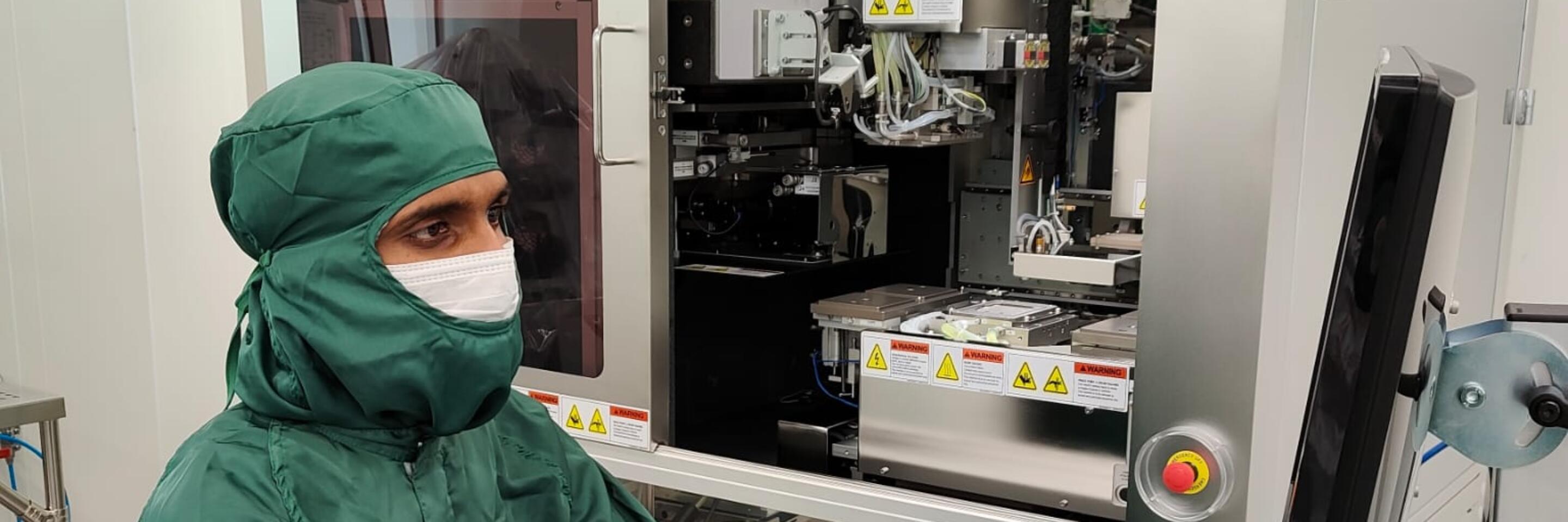
AdvaFab provides a commercial flip chip service for our customers’ high-value components. In addition to production-oriented work, R&D services are available based on customers’ needs.The AdvaFab team has been involved in flip chip bonding of hybrid pixel detectors with various sensor materials since 2002 developing special competences. The team composes of professional who have solved a great number of technological issues.
-
The typical sensor materials flip chip bonded are Si, GaAs and Cd(Zn)Te. These materials can be flip chip bonded up to chip thickness of 5 mm. The minimum size 4 mm x 4 mm and the maximum ASIC size is 5 cm x 5 cm. The sensors can be, however much larger as they can be moved on the bonding chuck after each flip chip placement. AdvaFab’s process suits for FC bonding of semiconductor/compound semiconductor chips with high interconnect density.
-
Rework means de-bonding the hybrid and removing the ASIC from the sensor chip to swap the malfunctioning chip to a functioning. The typical reason for rework is to replace the ASICs with hidden flaws that weren’t caught by the wafer-level probing. In the rework process, the sensor module will be heated well above the melting point of the solder alloy and the ASIC will be pulled off from the sensor. The rework process is a very valuable, because it will reduce very expensive silicon waste. It is particularly important for large monolithic Si/CdTe/GaAs sensors where several ASICs have been flip chip bonded on the sensor where the probability of a flawed ASIC or interconnects has been increased. The rework process is available for Si/GaAs/Cd(Zn)Te sensor materials. The rework can be done if the sensors have been kept in clean room environment and the modules haven’t been clued or contaminated in other ways.
-
The modules are typically delivered safely in vacuum-release trays.
-
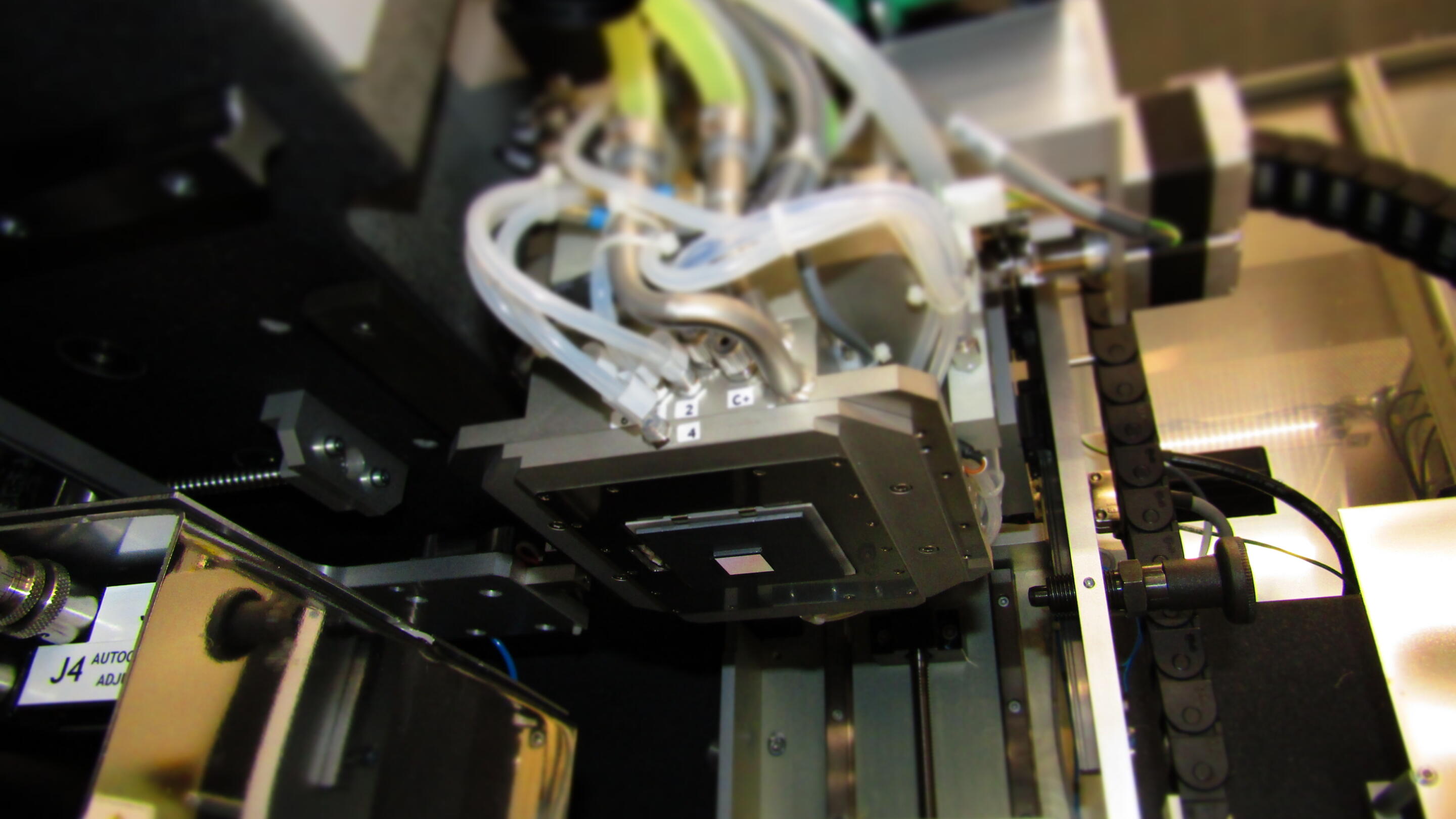
Flip chip bonding arm holding an ASIC.
-
-
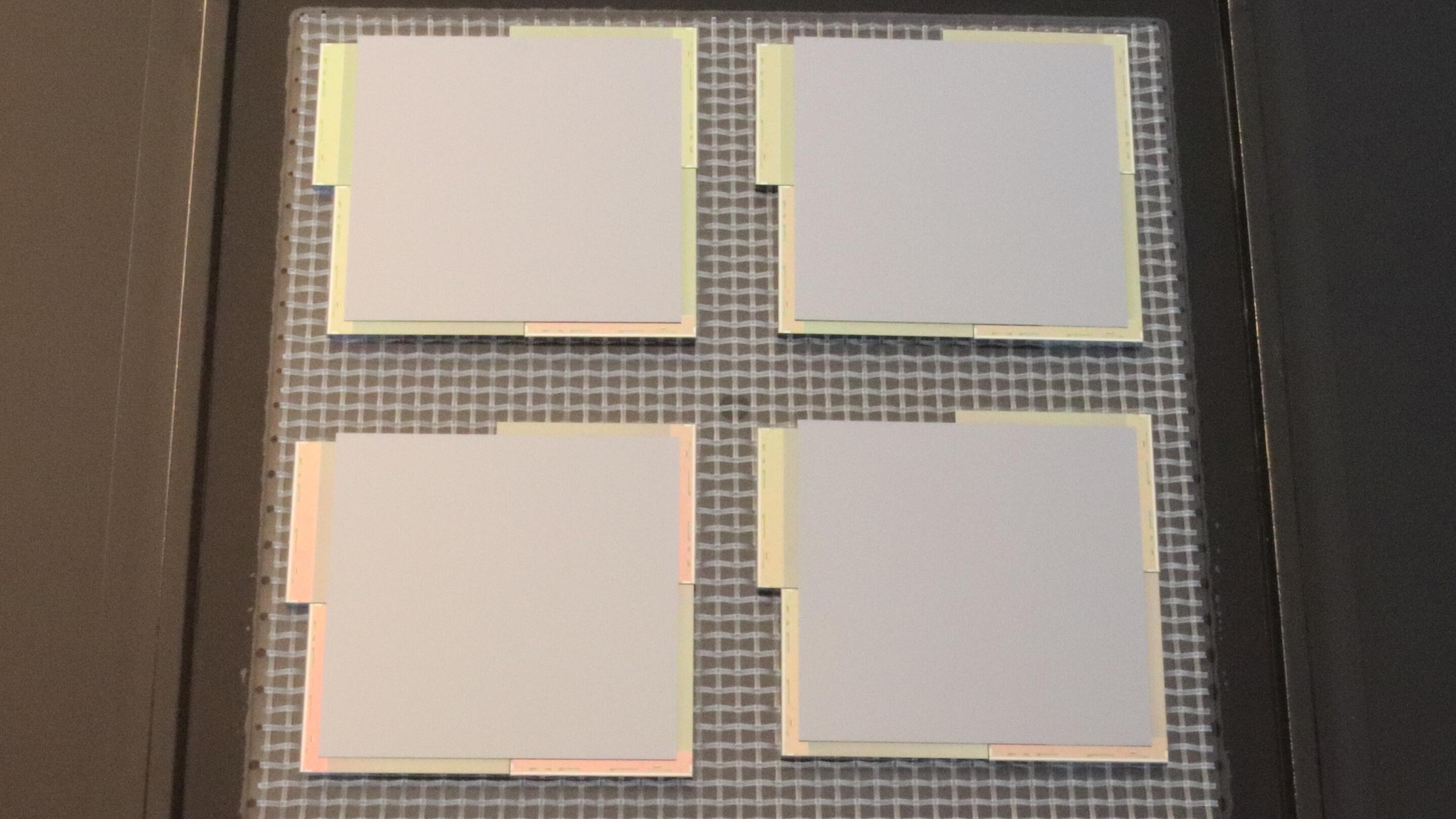
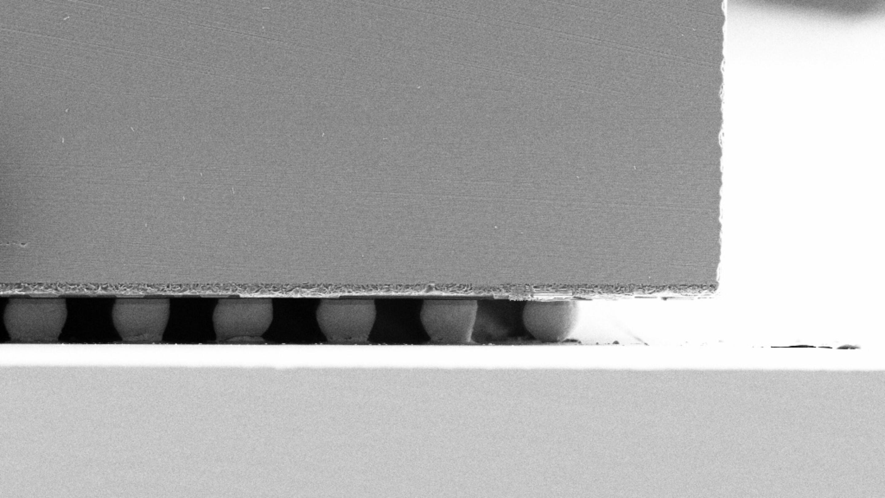
A quad modules with a compound semiconductor sensor on the top and four flip chip bonded ASIC at the bottom.
-
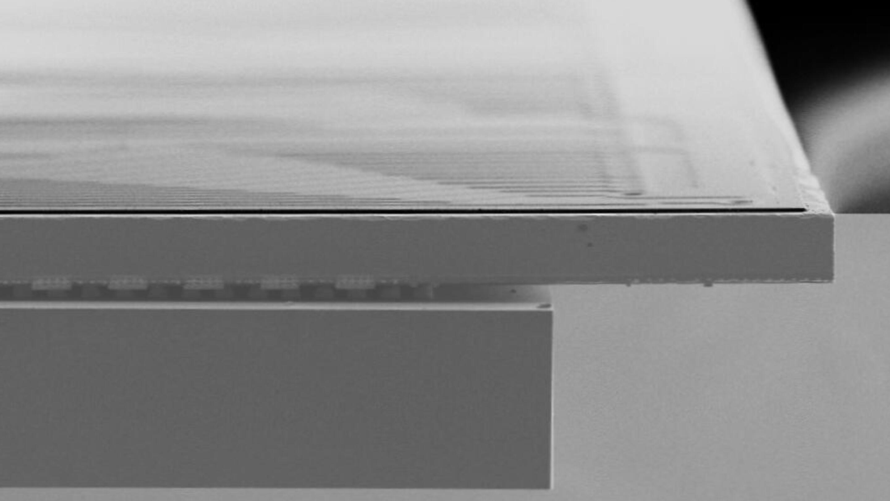
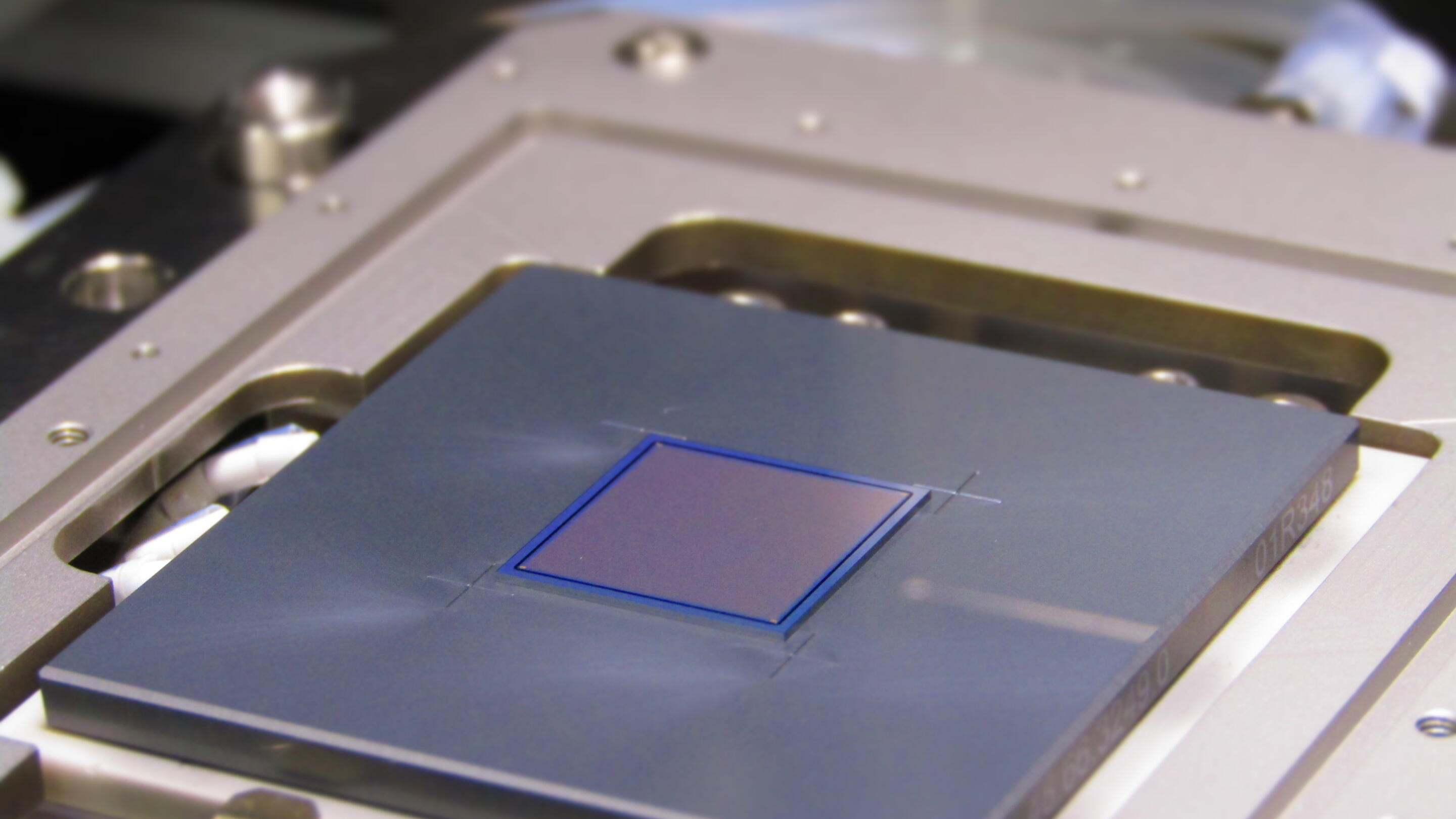
Thin ASIC with Through Silicon vias bonded to a 300 um thick edgeless Si sensor at AdvaFab
-
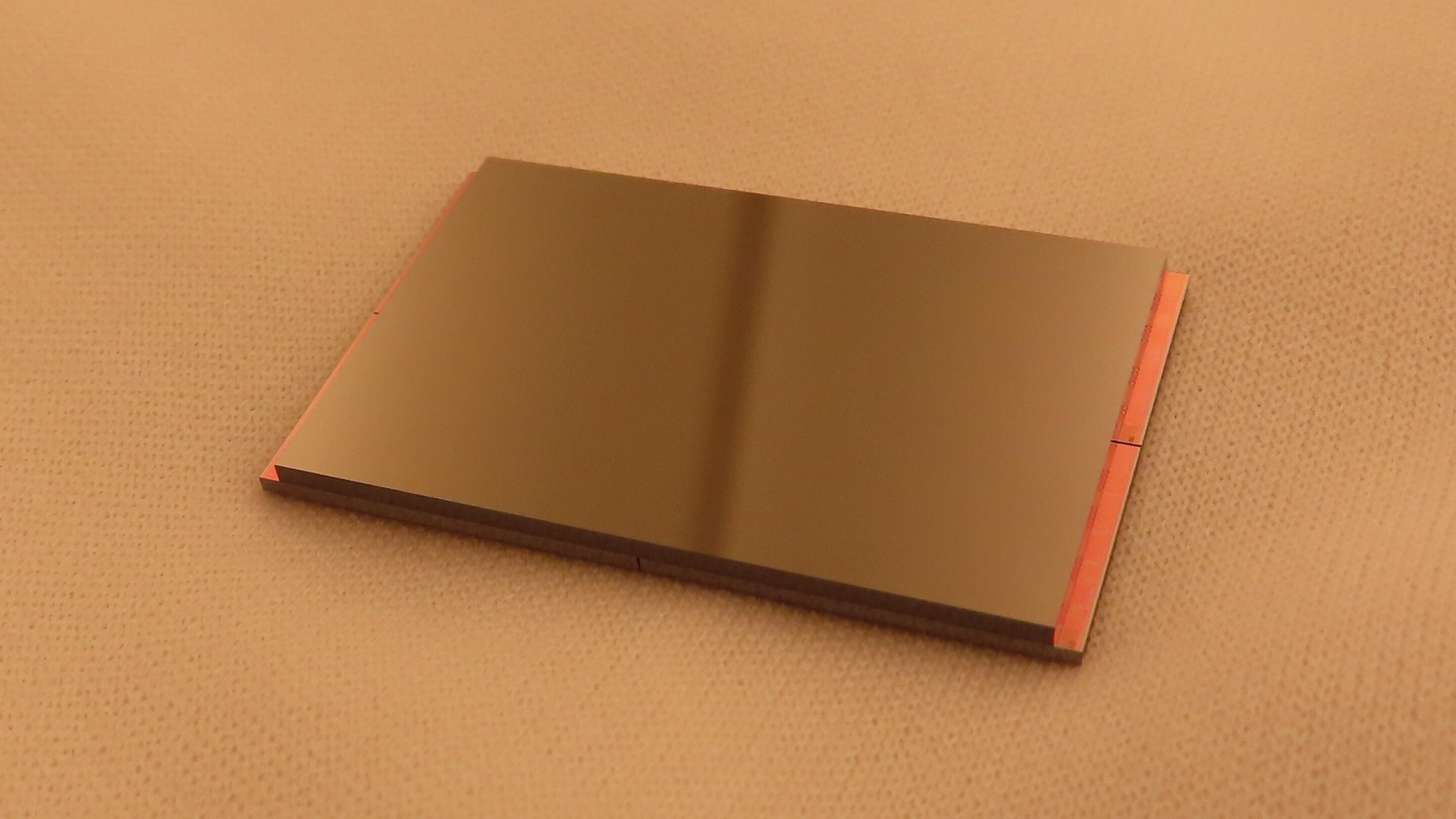
Flip chip bonded CdTe pixel sensor module.
Enhance Your Devices with Our Next-Generation Semiconductors
Join the ranks of the most advanced technology users with our cutting-edge solutions
Our Services – We offer full service catalog from design to production
We offer a comprehensive suite of semiconductor services, expertly crafted to meet the demands of both small and large-scale productions as well as the most ambitious research & development projects.


