Mask Design for Sensor Manufacturing and ASIC Wafer Bumping
Advafab’s mask design service exploits the manufacturing experiences gained over tens of years. The well-designed masks facilitate the fabrication process and also increase the yields.
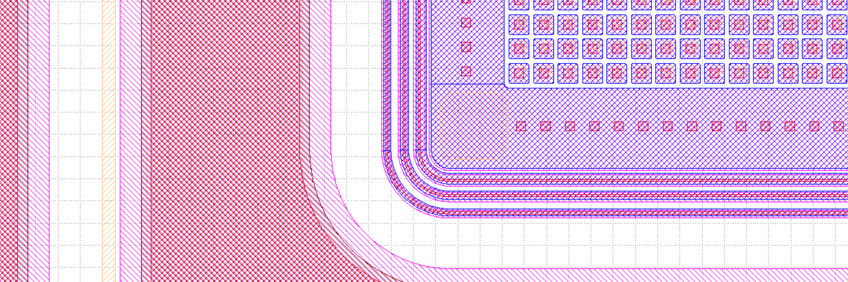
Advafab does mask design for sensor wafer processing, under bump deposition and bumping of the ASIC wafers. The service is available for the company’s customers. We design both contact masks and stepper reticles.
-
AdvaFab uses stepper lithography for Si sensor manufacturing. The reticles have been designed to allow manufacturing of various sensor geometries using the same reticle mask set. It is a flexible and cost efficient methodology for manufacturing Si sensor wafers for small and large batches.
The benefit of the stepper lithography is a superior yield compared to the conventional contact mask lithography in terms of defects and feature conformity over the wafer area.
-
Soda-lime or quartz-based wafer-level mask plates are used for the UBM deposition of the sensor wafers that have unknown process history.
The contact masks are typically applied for sensor wafers fabricated by third party foundries. Each wafer layout requires its own mask plate, which increases the fabrication costs.
-
Wafer bumping process requires only one contact mask plate. For the preparation of the ASIC wafer-level bumping mask, the customer should deliver the reticle level layout and stepping information of the top most metal and passivation layers. The wafer-level layout, alignment marks and dummy bump structures will be designed to optimize the electroplating uniformity on the wafers. Complete wafer layouts are preferred if the layouts have been proven to work in the production.
Typically, visible “Bump ID” patterns are designed at the periphery of the chips to obtain visible ID marks after the bumping process. The bump id marks can be seen using an optical microscope and they have turned out to be very valuable to confirm that the right ASICs have been used for the flip chip bonded sensor modules.
Our Services – We offer full service catalog from design to production
We offer a comprehensive suite of semiconductor services, expertly crafted to meet the demands of both small and large-scale productions as well as the most ambitious research & development projects.


