Dicing of Wafers
“Every cut matters” describes Advafab’s philosophy in dicing of fragile semiconductor wafers. Care and patience must be shown when delivering high-quality dicing with minimal chipping.
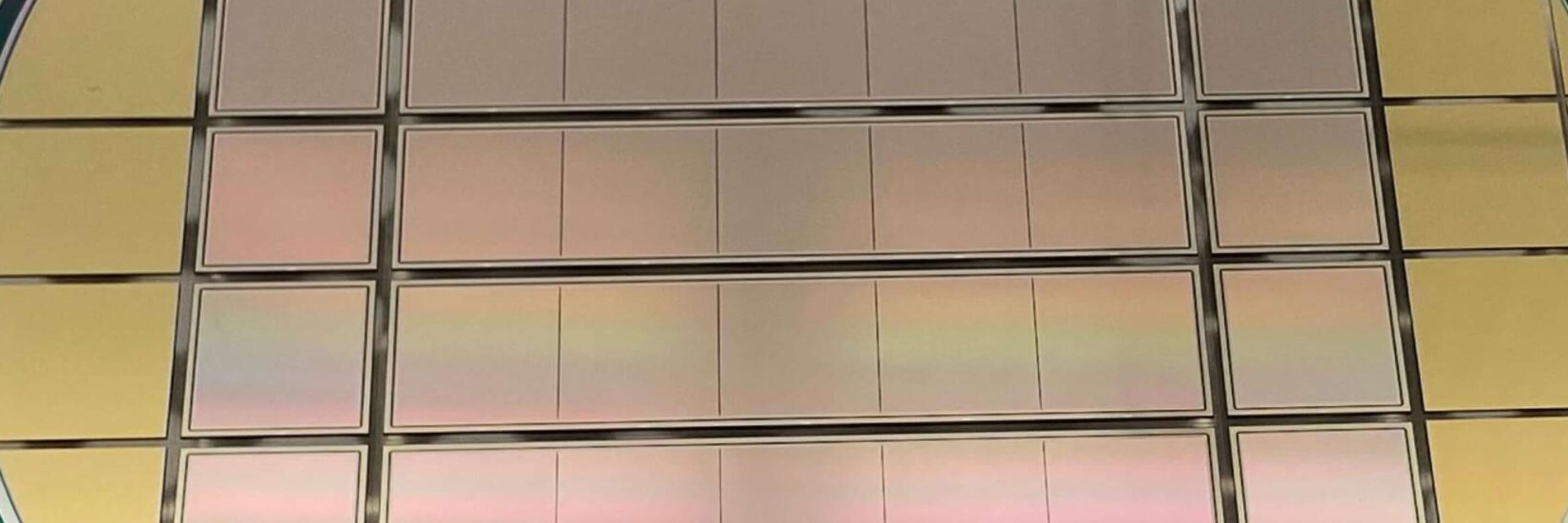
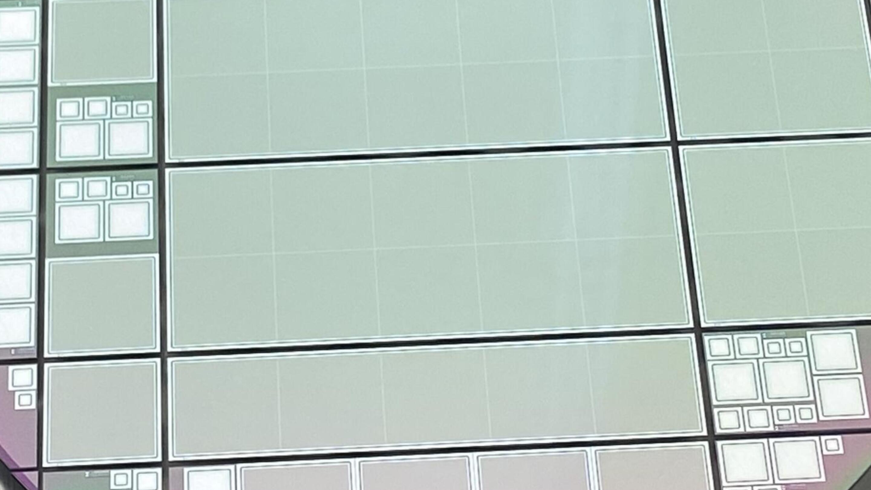
Over the years AdvaFab has developed special competence in dicing of the sensor and ASIC wafers. Dicing processed have been established for typical sensor materials including Si, GaAs and Cd(Zn)Te. Moreover, there are processed for dicing fused silica and quartz wafers. All the dicing processes are based on diamond blade dicing and our approach to dicing is minimise the amount of chipping instead of looking for high throughput processes.
-
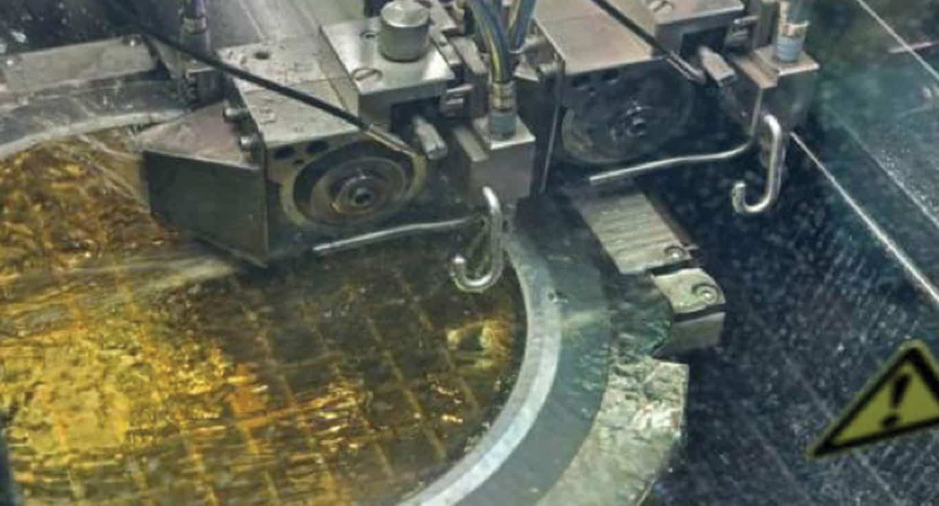
Dicing saw in action
-
The compound semiconductors are challenging materials to be diced. Special dicing blades and dicing parameters are required for the materials.
-
Enhance Your Devices with Our Next-Generation Semiconductors
Join the ranks of the most advanced technology users with our cutting-edge solutions
Our Services – We offer full service catalog from design to production
We offer a comprehensive suite of semiconductor services, expertly crafted to meet the demands of both small and large-scale productions as well as the most ambitious research & development projects.


