Semiconductor Pixel Sensor Modules
A pixel sensor module is a device that incorporates a pixel image sensor with associated circuitry into a single module.
Semiconductor pixel sensors are electronic devices that convert radiation into electrical signals to capture images or video. The semiconductor sensors are manufactured from Silicon, Gallium Arsenide or Cadmium (Zinc) Telluride materials.
The Semiconductor pixel sensor modules are highly versatile and find applications in a wide range of imaging systems. Their integration into modules simplifies the design and integration process, making them an essential component in modern imaging technology.
-
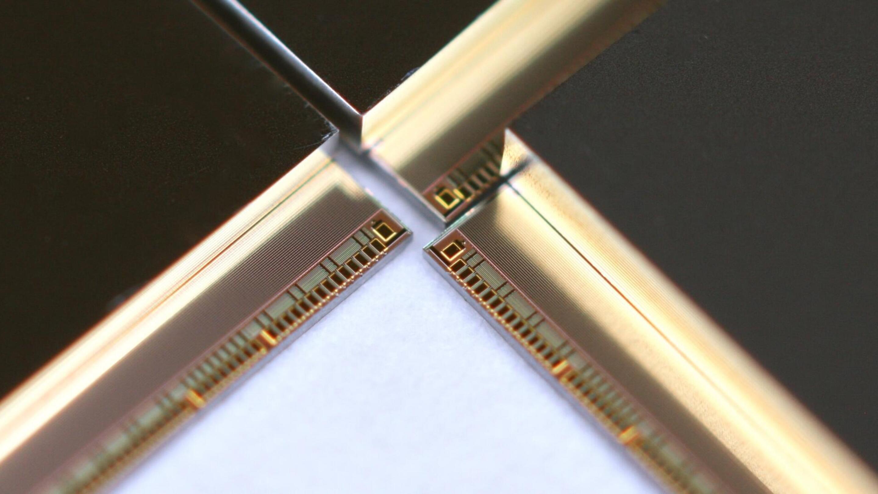
Edgeless Silicon through-silicon-via pixel sensor modules produced at Advafab.
-
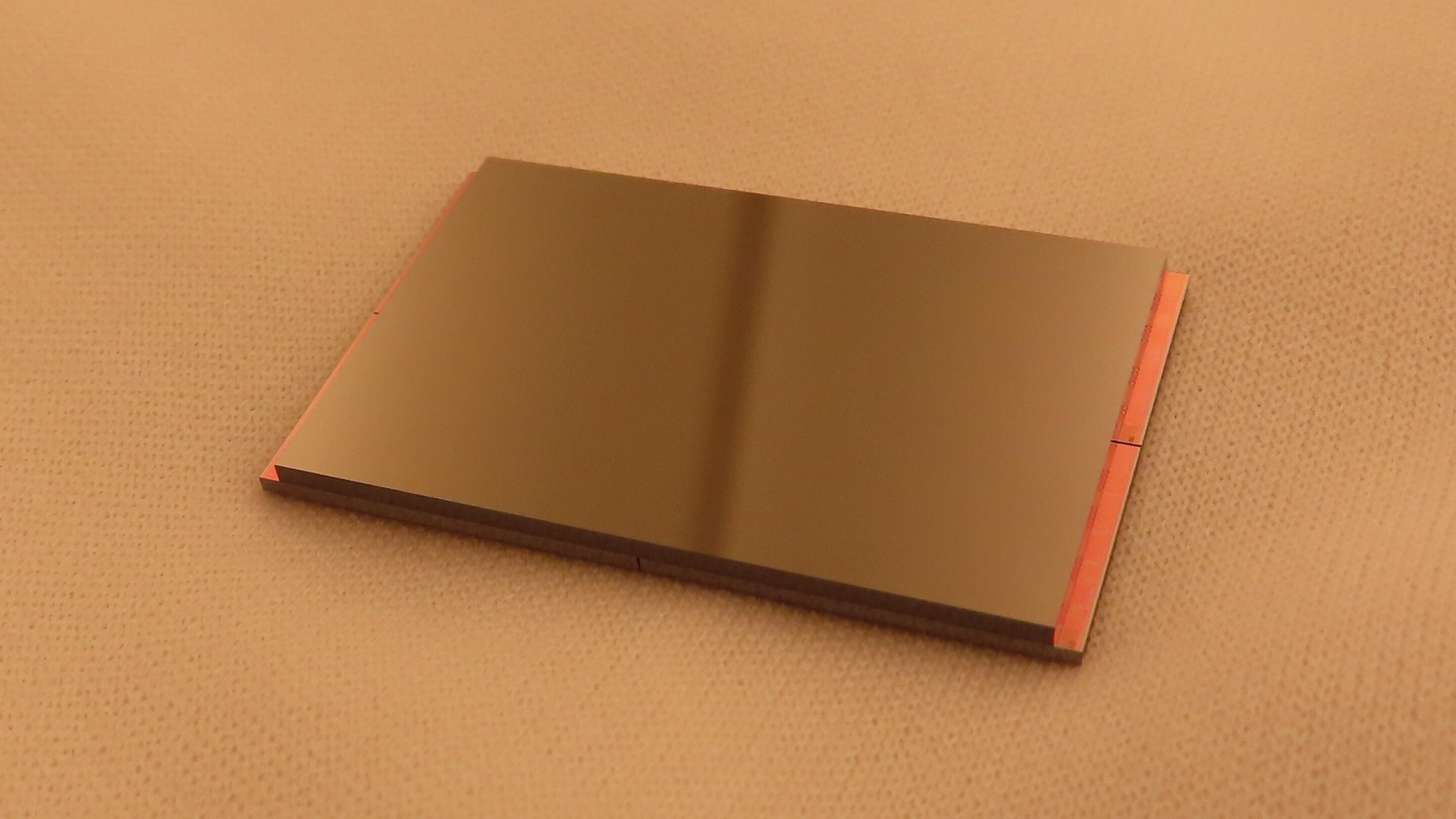
Flip chip bonded 2 mm thick CdTe sensor module.
-
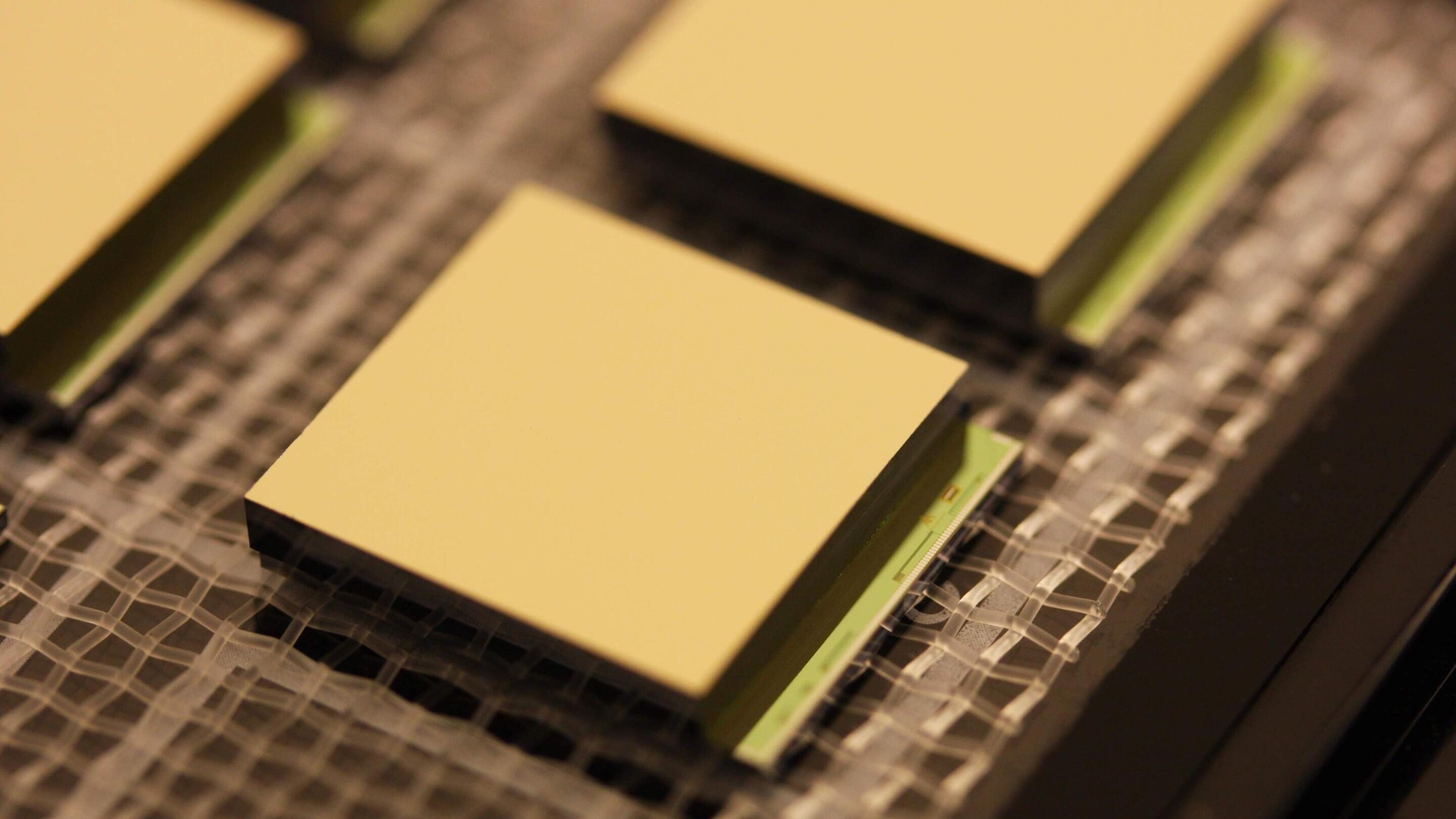
A quad modules with a compound semiconductor sensor on the top and four flip chip bonded ASIC at the bottom.
-
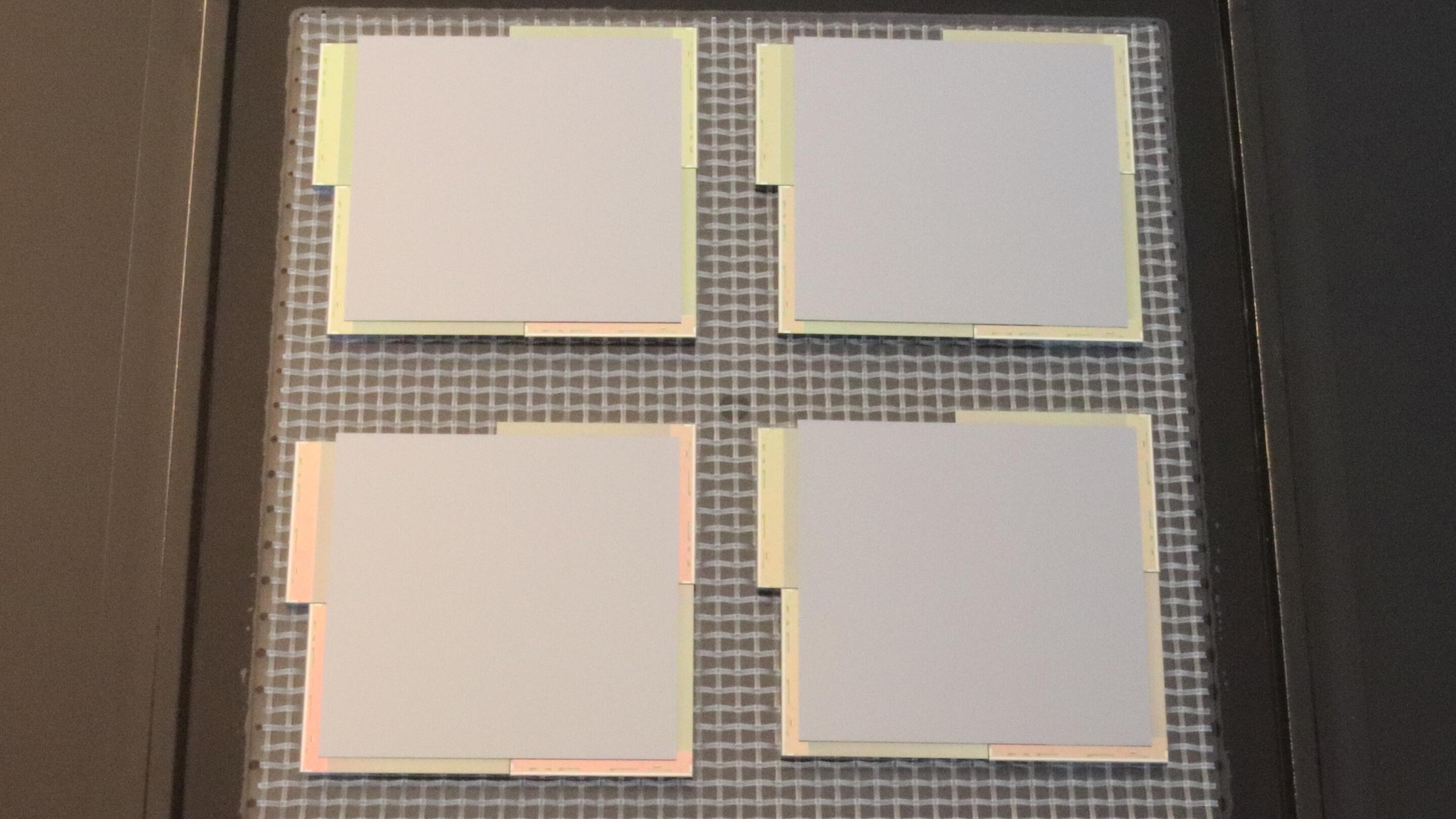
The modules are typically delivered safely in vacuum-release trays.
Pixel Sensor Module Technology
Advafab provides semiconductor pixel sensor modules based on direct conversion technology.
The term direct conversion refers to immediate conversion of the X-rays into electric charge within the semiconductor crystal with a known semiconductor sensor material dependent conversion rate. The direct conversion technology is necessary to record the energy of the incident radiation accurately in spectral imaging applications.
-

Cross section of two pixels of the semiconductor pixel sensor module.
-
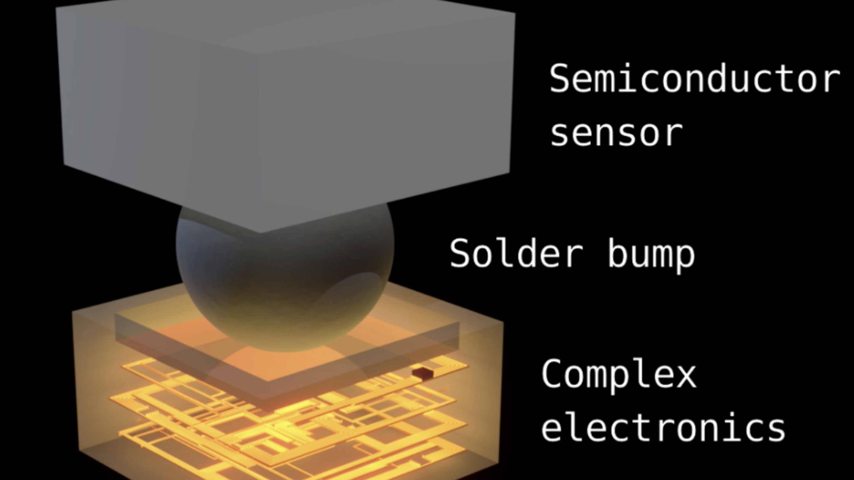
Single pixel of the semiconductor pixel sensor module.
Pixel Sensor Module Operation Principle
Advafab’s pixel sensor module detects the incoming radiation by directly converting the energy of the radiation into electric signal.
The readout circuitry is reading out the electrical signals generated by the pixels of the semiconductor sensor. The readout circuitry amplifies, digitizes, and processes the analog signals into digital data that can be further processed or stored. The readout circuitry can be either based on photon counting or charge integrating.
Illustration of the operation principle of a single pixel when an incoming X-ray is detected and how the direct conversion pixel sensor modules maintain a high spatial resolution.
Pixel Sensor Module Quality
Advafab delivers conforming high-quality modules to its customers.
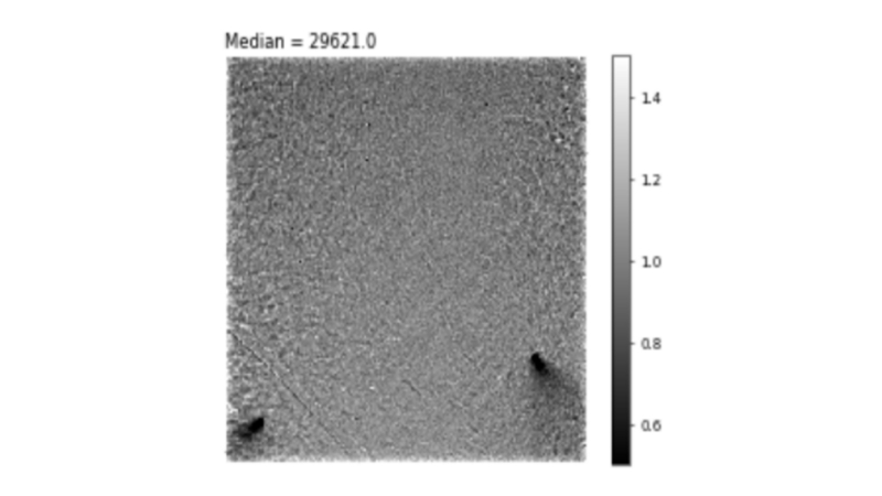
The conformance of the pixel sensor module is verified using X-ray probing technique, where the module is irradiated by X-ray fluorescence radiation and module response is recorded to evaluate both the flip chip bonding quality and the sensor operation. The X-ray probing is currently available for Timepix1, Timepix3 and Medipix3 readout ASIC electronics.
-
Silicon is a uniform and stable sensor material thus the focus of the Si pixel sensor module conformance measurement is on the flip chip bonding quality, i.e. the number of non connected pixels, and the operation of the ASIC electronics.

-
GaAs is a stable but less uniform sensor material than Silicon. The focus of the GaAs pixel sensor module conformance measurement is on the uniformity, flip chip bonding quality, i.e. the number of non connected pixels, and the operation of the ASIC electronics.
-
CdTe is unstable and less uniform sensor material than GaAs. The focus of the CdTe pixel sensor module conformance measurement is on the stability, uniformity, flip chip bonding quality, i.e. the number of non connected pixels, and the operation of the ASIC electronics.

Assembling of Pixel Sensor Modules
Advafab works closely with its trusted partners to offer small to large-scale PCB-level assembling of the pixel sensor modules.
Advafab’s customers are able to outsource the design and manufacturing of the PCBs together with mounting and wire bonding of Advafab-manufactured conforming products on the PCB.
Semiconductor Materials for Pixel Sensor Modules
Each of these materials has its own unique properties and advantages, which make them suitable for different applications.
Our Services – We offer full service catalog from design to production
We offer a comprehensive suite of semiconductor services, expertly crafted to meet the demands of both small and large-scale productions as well as the most ambitious research & development projects.


