Usage of GaAs Sensors
Gallium Arsenide (GaAs) sensors are used to detect X-rays, γ and electrons in a medium energy range, where the Si absorption efficiency is not sufficient.
GaAs sensors offer advantages such as high electron mobility, high sensitivity, high density, low energy X-ray fluorescence photons and radiation hardness, making them suitable for various applications. Here are some typical energy ranges and applications where GaAs sensors are employed:
- Medium-Energy X-rays: GaAs sensors can effectively detect and measure X-rays up to 60-80 keV depending on the sensor thickness. This includes applications such as medical soft tissue X-ray imaging, non-destructive testing of light-weight materials, small animal imaging, X-ray diffraction, X-ray spectroscopy, and gamma-ray detection
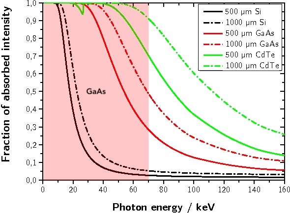
X-ray absorption in GaAs sensor and its usable energy range. Source publication
- High-Energy electrons: GaAs sensors can effectively detect and measure electrons due to its high density in energy range from a few keV to few of MeV. This includes applications such as Transmission Electron Microscopy (TEM) and Electron Energy Loss Spectroscopy (EELS)
- Medium Energy particles: GaAs sensors are also utilized in the medium-energy range for the detection of accelerated particles, typically in the tens of megaelectronvolt (MeV) range. The GaAs sensor are used for radiation detection and measurement in applications such as radiation therapy, nuclear medicine, environmental monitoring for radioactive materials, high-energy physics and cosmic ray experiments.
- High Energy particles: GaAs sensors are employed in high-energy physics experiments, such as particle colliders and cosmic ray experiments, where particles with energies ranging from billions of electronvolts (GeV) to trillions of electronvolts (TeV) are detected. These sensors enable the tracking and measurement of high-energy particles produced in these experiments.
GaAs Semiconductor Material
Gallium Arsenide (GaAs) is a compound semiconductor material composed of gallium (Ga) and arsenic (As) atoms.
GaAs belongs to the III-V group of semiconductors, which means it is formed by elements from Group III (Gallium) and Group V (Arsenic) of the periodic table. GaAs is a direct bandgap semiconductor, meaning it can efficiently absorb photons and convert them into electrical signals.
Gallium (Ga): Gallium is a soft, silvery metal with atomic number 31. It is a post-transition metal and is known for its low melting point, which makes it useful in certain applications.
Arsenic (As): Arsenic is a metalloid element with atomic number 33. It is known for its toxicity, but in compound form, such as in GaAs, it is chemically stable and safe to handle. Arsenic contributes to the semiconducting properties of GaAs, including its energy band structure and electrical conductivity.
GaAs is available in small (50 mm) to medium (150 mm) size wafers; the material is commercially available in different grades; its price is affordable; it has a good uniformity and material integrity compared to Cd(Zn)Te.
-
Gallium Arsenide (GaAs) is not found naturally in significant quantities in the Earth’s crust. It is considered a synthetic compound, meaning it is produced through human manufacturing processes rather than occurring naturally.
Both gallium (Ga) and arsenic (As) are elements that can be found in nature, but they do not exist in their pure forms as GaAs. Gallium is a relatively rare element and is often found as a byproduct of mining and refining other metals, such as aluminum and zinc. Arsenic, on the other hand, is more abundant and can be found in various mineral ores, such as arsenopyrite and realgar.
-
Semiconductor-grade GaAs is grown as ingots using different techniques. The growth technique has a major contribution to the number of impurities. Several methods are employed for GaAs crystal growth, including the following:
- Vertical Bridgman (VB) Method: In the VB method, high-purity GaAs feedstock is placed in a sealed ampoule or crucible. The ampoule is heated, causing the GaAs to melt. A seed crystal of GaAs is immersed in the molten material, and the ampoule is slowly moved upwards or downwards (vertically) through a temperature gradient. As the ampoule moves, the GaAs crystal grows on the seed crystal due to the slow cooling process. The resulting crystal is a single crystal ingot with a cylindrical shape.
- Liquid Encapsulated Czochralski (LEC) Method: The LEC method involves a similar process to the Czochralski method used for silicon crystal growth. In this method, a high-purity GaAs feedstock is melted in a crucible. A seed crystal of GaAs is dipped into the molten material, and it slowly withdraws from the melt while rotating. As the seed crystal is pulled out, GaAs crystallizes on the seed crystal surface, forming a single crystal ingot. The molten GaAs is “encapsulated” in a liquid gallium arsenide solution to provide controlled conditions for crystal growth.
- The Vertical Gradient Freeze (VGF) method is used for the growth of Gallium Arsenide (GaAs) crystals. In this technique, a high-purity GaAs feedstock is melted in a crucible. A seed crystal is inserted into the molten material, and the crucible is slowly lifted or moved while maintaining a controlled temperature gradient. As the temperature decreases, the molten GaAs solidify on the seed crystal, resulting in the growth of a single crystal GaAs ingot. The VGF method allows for the production of larger GaAs crystals compared to other methods.
Learn more about other Semiconductor Materials
Enhance Your Devices with Our Next-Generation Semiconductors
Join the ranks of the most advanced technology users with our cutting-edge solutions