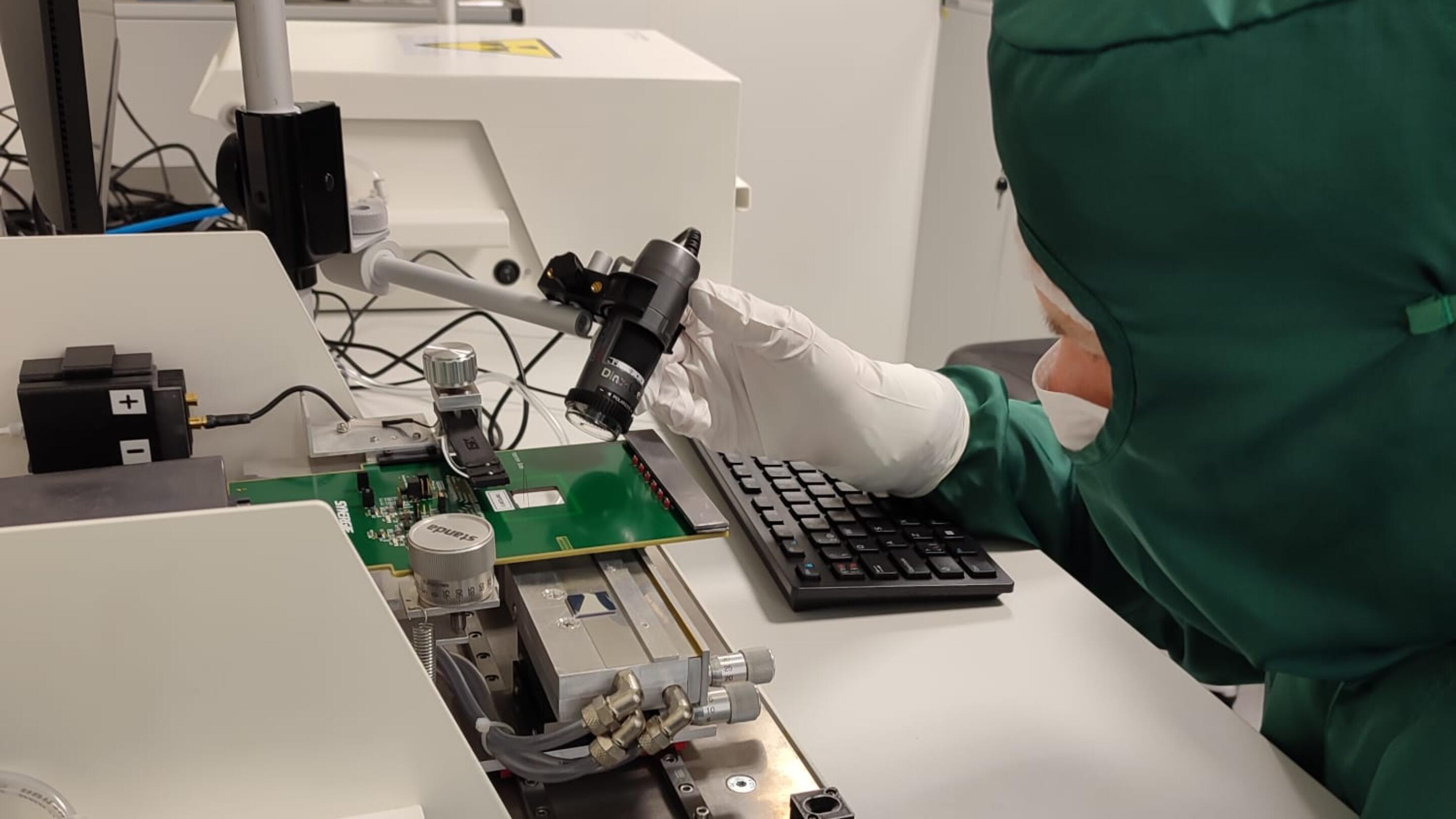
Sensor Module Level X-ray Probing
Probing of the modules under X-ray fluorecense photons allows full characterization of the flip chip bonded Si, GaAs and CdTe modules.
AdvaFab has three X-ray probers for testing of Timepix1, Timepix3 and Medipix3 sensor modules. It is possible identify the flip chip bonding quality, functionality of the ASIC, stability of the sensor and see intrinsic defects in the sensors on every module before delivering it to our customer. Moreover, the stability of the pixels can be measured over time. The sensor is irradiated by fluorescence photons of the target. Available targets are Fe (6 keV), Cu (8 keV), Cd (23 keV) and In (24 keV).
The detailed module-level testing enables us to confirm the quality of the modules before dispatching them to our customers. If the tested module is bad, we will repair it on-site and reduce the costs of bad quality. Because of the improved testing our customers will save labour and materials and logistics costs. The X-ray probing process doesn’t cause any mechanical damage to the sensor chips.
-
ASIC readout chip is digitally tested to identify digitally bad pixels or columns.
The matrix of random numbers is loaded into the chip (one number to one pixel) and then it is read out from the chip and compared. If the input matrix corresponds to the output matrix then all pixels are digitally working. The maximum number of bad responding pixels is set at 65.
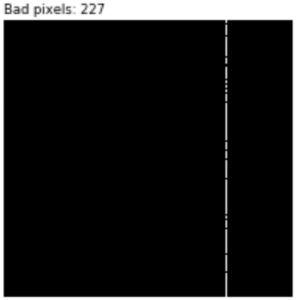
Example of a digital test identifying a bad pixel column in the ASIC. -
The threshold is set far from the noise edge. Bias voltage is increased in steps and the number of noisy pixels is evaluated. Pixel is signed as leaking if it is noisy in more than 50% of acquisitions. In the case of CdTe sensors, the bias voltage is applied a certain time before the measurement begins to stabilize the current level. The leakage current can be compared with values measured by the third party sensor manufacturer. The precision of measurement is 0.5 µA with Timepix1 and Medipix3 and 1.5 µA with Timepix3. After this test a default bias voltage is set.

Example of a leakage current test of a compound semiconductor sensor identifying a breakdown of the sensor at 240 V. -
All pixels in the Timepix/Medipix chips are designed to be identical. However, due to CMOS processing some parameters may vary from pixel to pixel. In particular, the local pixel threshold value is slightly different from pixel to pixel. The threshold (THL) equalization is a procedure that sets adjustments for each pixel and makes the overall threshold level as homogenous as possible.
Among the observed parameters belong to the shape of histogram peaks, their positioning, and continuity. The width of the average of the threshold distribution refers to the low dispersion value – standard deviation. The main output parameters of the equalization are following:
- Mean THL [ADU] corresponds to the average value of final threshold distribution (mean value of the green peak in Picture 3). This value serves as an input for calculation of the minimal threshold during the threshold calibration procedure.
- Std.Dev (standard deviation) shows the dispersion of the average threshold distribution.
- Final THL [ADU] is calculated as a multiple of sigma which is added to the Mean THL Value. This calculated value helps to determine the minimum threshold value. This threshold value indicatively [ADU] defines the noise edge. It means the value where no pixels are noisy.
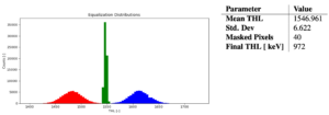
Example of a completed Timepix3 threshold equalization. -
The aim of this test is to determine the suitable bias voltage for the sensor operation. The bias voltage is scanned over a predefined range and the response of the sensor is measured. The voltage range and step depend on the sensor type and thickness. For each bias voltage, the sensor is irradiated by fluorescence photons. The measurement is performed in Frame or Integral mode based on sensor type. The number of detected counts is added to the plot labeled “Count rate vs. bias”.

The full depletion voltage
of the sensor is typically at the voltage where the count rate reaches 80% value.The measured count rate is related to the degree of depletion of the sensor material. When the bias voltage is low, the depletion zone begins from the pixel side and proceeds towards the continuous electrode along the increased voltage. If the sensor volume is not depleted, the sensor does not detect low-energy X-rays depositing their charge in the proximity of the continuous electrode of the sensor. By increasing the bias voltage, the count rate increases linearly until it plateaus at full depletion voltage. At this point, the measured frames become homogeneous. Further increase in the bias voltage does not have any significant influence on the acquired images.
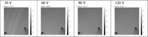
Image of bias scans of a 500 um thick Si sensor. The radial lines at 30 V bias voltage are caused by the resistivity variation in the silicon ingot. The operational range of the module is given by the count rate plateau. The optimal bias voltage is determined based on the sensor material and thickness. The bias test is performed to verify that the selected bias value is within the operational range.
-
stability test is aimed to determine the sensor stability over time evaluating the number of deviating pixels and the instabilities of the entire sensor volume. The measurement is performed in the Frame mode. One frame is acquired for 20 seconds, the acquisition is repeated 30 times. That means, the total acquisition time is 10 minutes. First, each frame is normalised to its mean value. Then the relative noise matrix is calculated using the following equation for each pixel separately.

The Global Stability represents the instability of the entire sensor volume and is calculated by the following equation, where the average denotes the mean of all pixels in a frame.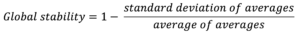
The sensor stability result is plotted as arelative noise matrix that represents the per pixel stability. The stability evaluation parameters and a histogram of the relative noise matrix are on the right side of the plot.
- Theoretical/ideal Median value of normalised picture is equal to 1.
- Pixel Median Range represents range for picture visualisation.
- The degree of pixel instability is evaluated using 2σ and 5σ intervals.
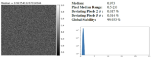
Example of a 10 min stability test of a 300 um thick Si sensor. -
The sensor bias voltage can be set up to 500 V. This may be an issue with thick Cd(Zn)Te (> 2 mm) sensors where a high depletion voltage needs to be applied to collect the charge from the whole sensor volume.
In some cases, the ASIC might behave strangely which makes the testing very challenging. In these cases, the goal of the sensor module X-ray probing is to take an X-ray image for the flip chip bonding quality conformance of the module.
-
Advafab offers four different types of quality conformance tests.
- No X-ray probing. Leakage current measurement of the flip chip bonded modules will be done up to 200 V for Si sensors fabricated at Advacam free of charge. For third-party manufactured sensors, the leakage current measurement can be done against a fee that is dependent on the measurement protocol.
- X-ray probing test including ASIC digital, leakage current, ASIC threshold equalization and sensor bias tests under X-ray fluorescence. This test doesn’t consist of a sensor stability test.
- X-ray probing with the sensor stability test.
- Customer-specific test for a special type of sensor or custom settings for the test.


Enhance Your Devices with Our Next-Generation Semiconductors
Join the ranks of the most advanced technology users with our cutting-edge solutions
Our Services – We offer full service catalog from design to production
We offer a comprehensive suite of semiconductor services, expertly crafted to meet the demands of both small and large-scale productions as well as the most ambitious research & development projects.


