Silicon Sensor Manufacturing
Advafab’s offering covers pixel, microstrip and diode sensors fabricated on 6” (150 mm) high resistivity silicon wafers having thicknesses from 200 µm to 1 mm. Even thinner sensors, down to a few micrometer thickness, can be fabricated using a well-established handle wafer SOI technology.
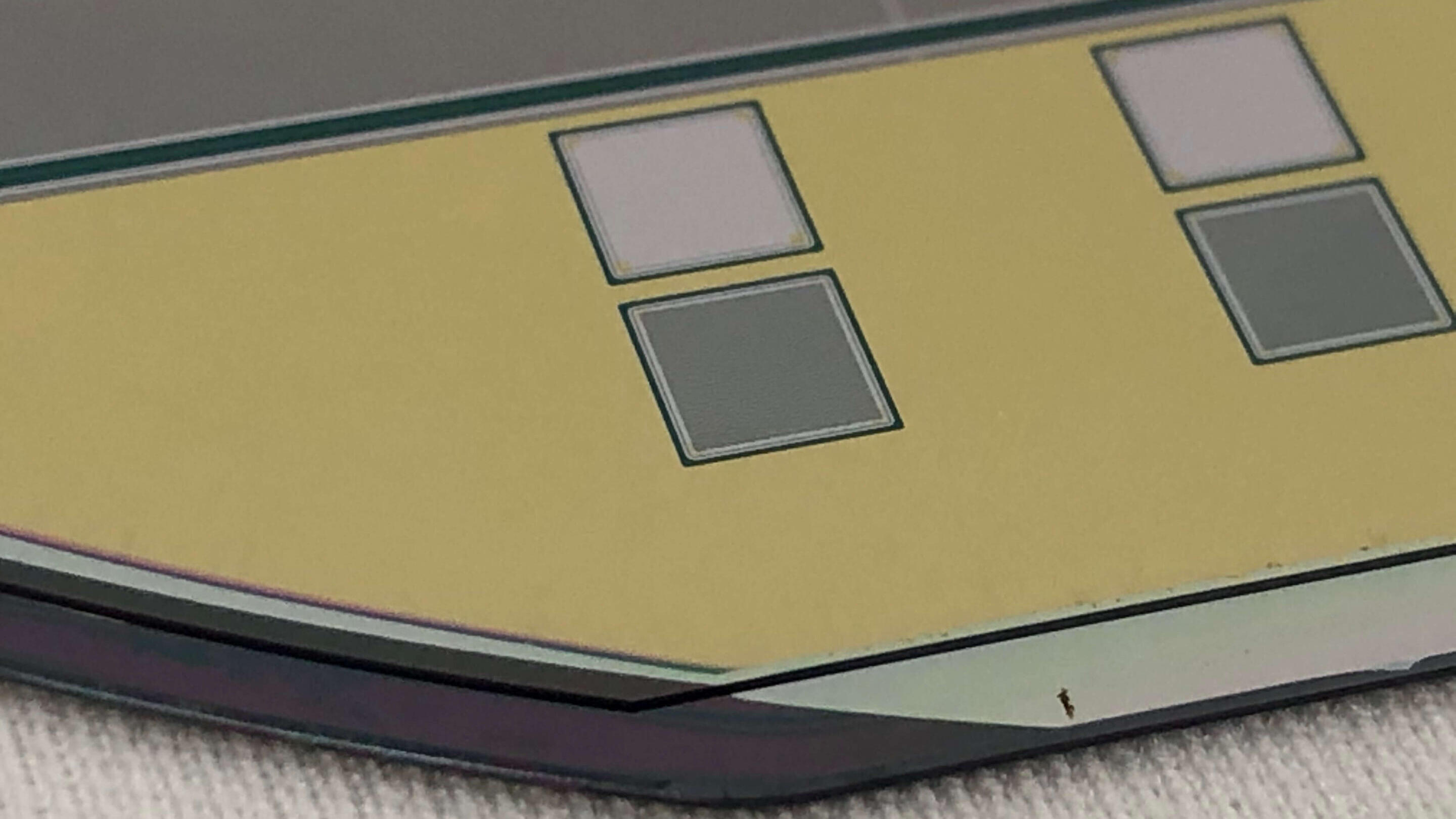
Planar Si sensor with any polarities, such as p-on-n, n-on-n, n-on-p and p-on-p can be fabricated. Both p-stop and p-spray technologies are available for the electrical isolation of the anode electrodes. The sensor processes both on 6″ and 8″ wafers provide low leakage currents and high breakdown voltages that are typically many times higher than the depletion voltage. The processing is carried out with a short delivery time. Advacam provides a possibility to continue the wafer processing by depositing the under bump metallization or solder bumps; carry out the dicing of the wafers and perform the flip chip bonding of the sensor modules. We also provide wire bonding of the flip-chip bonded assemblies to the PCB.
-
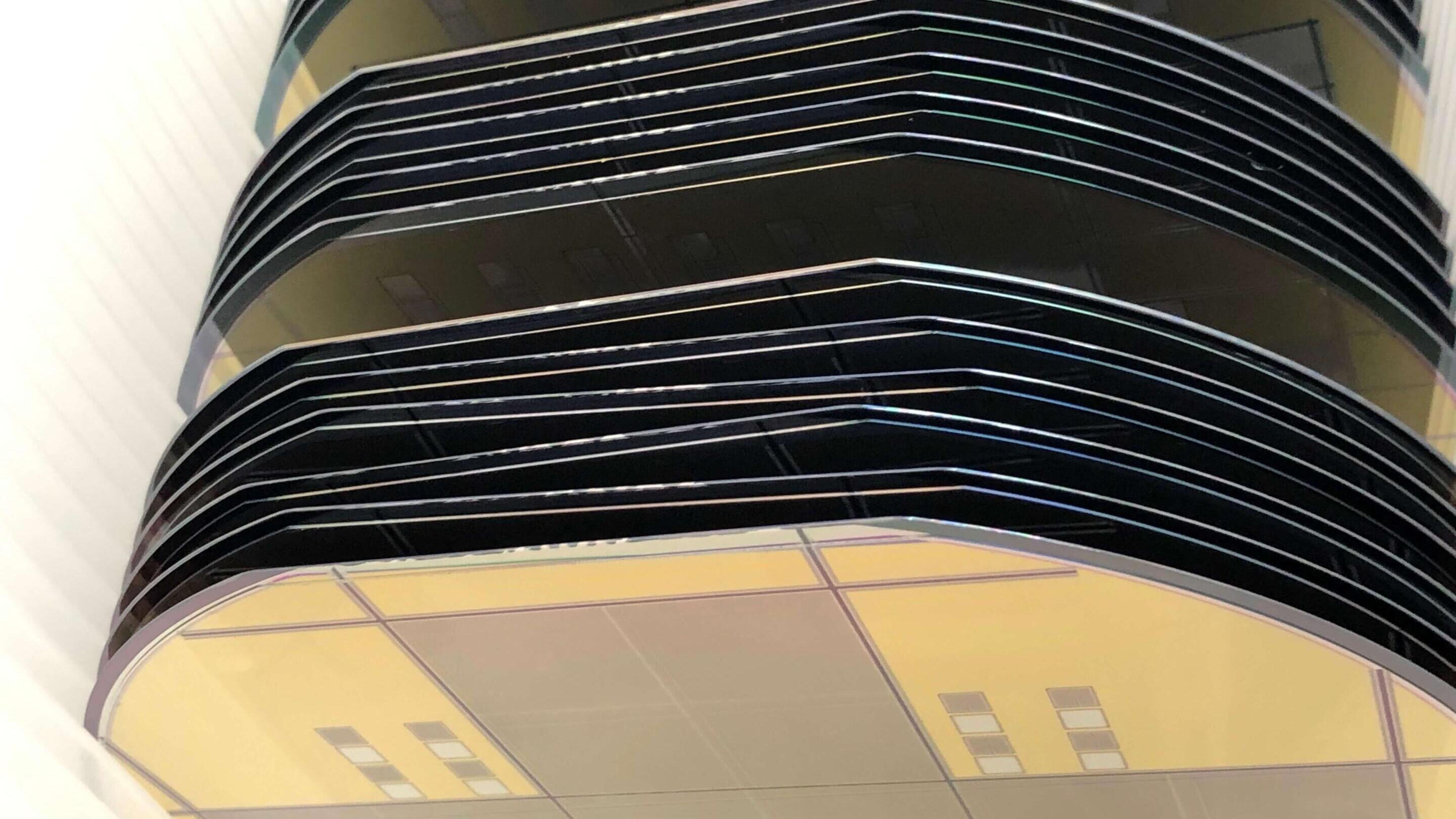
200 mm planar Si wafers entering to annealing furnace.
-
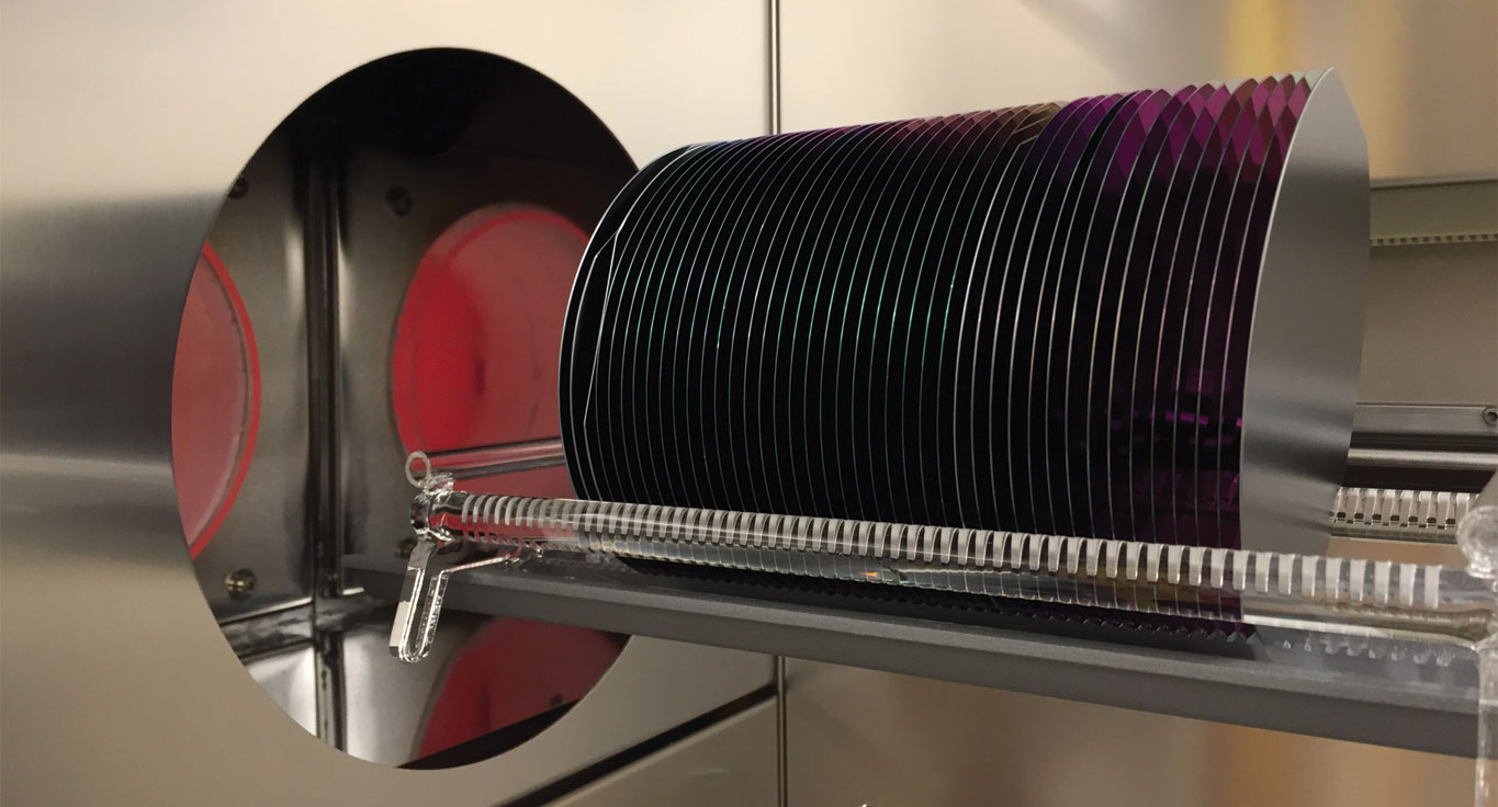
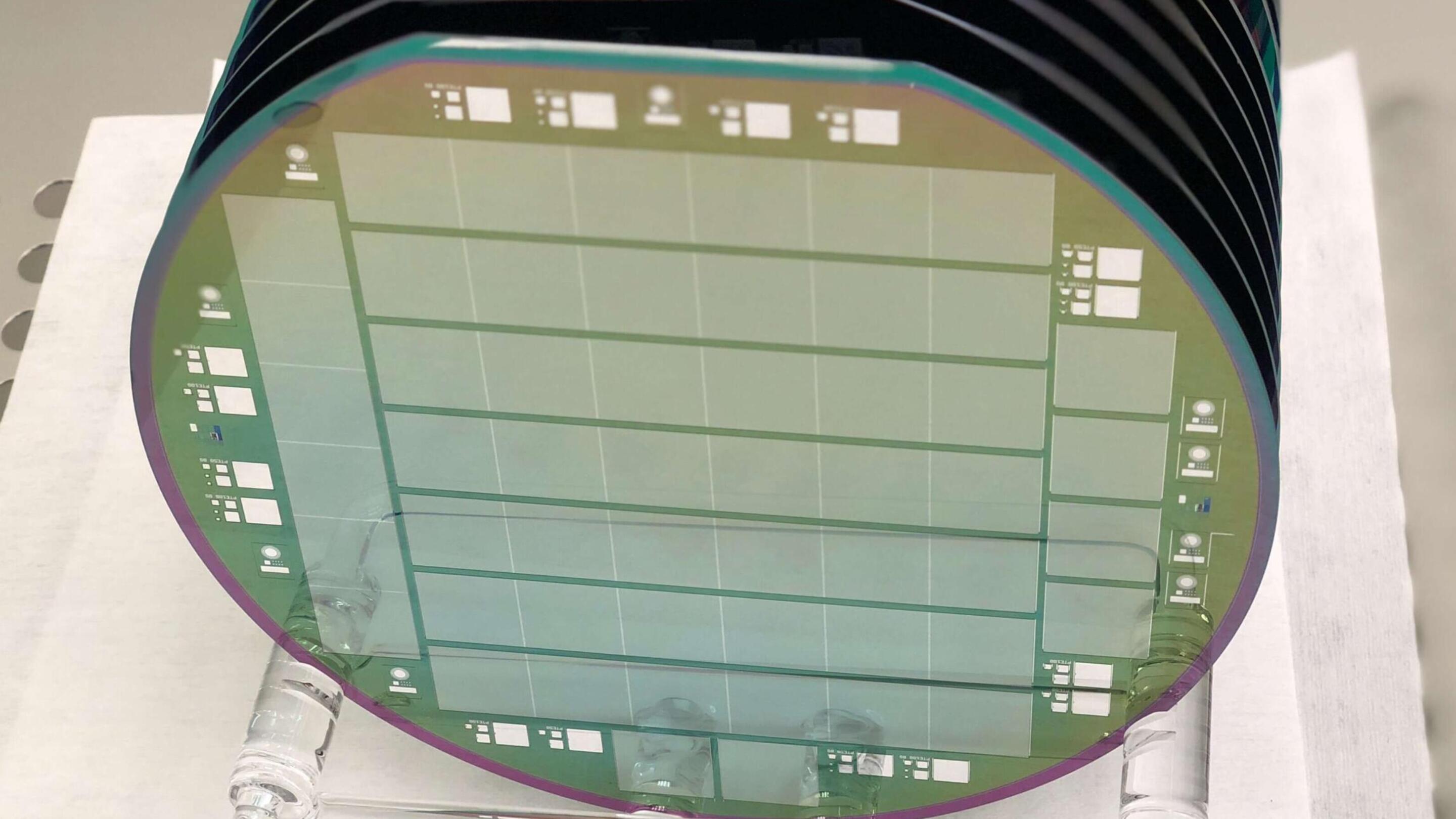
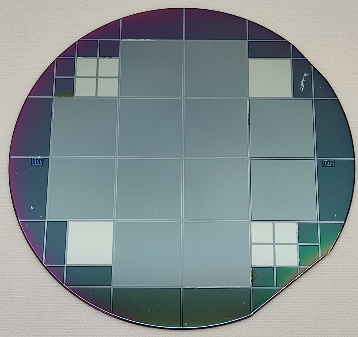
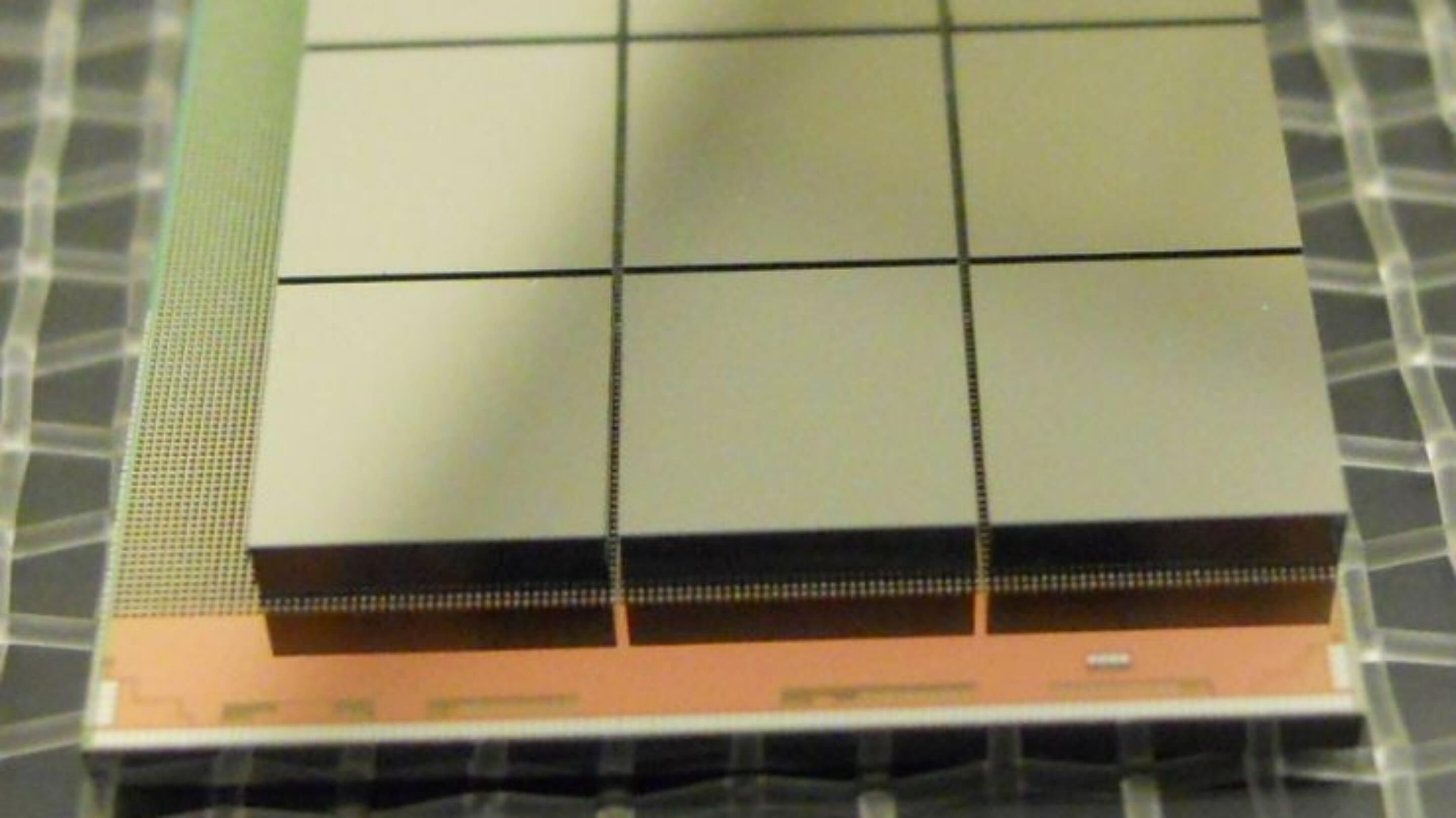
150 mm planar Si pixel sensor wafer manufacturing batch.
-
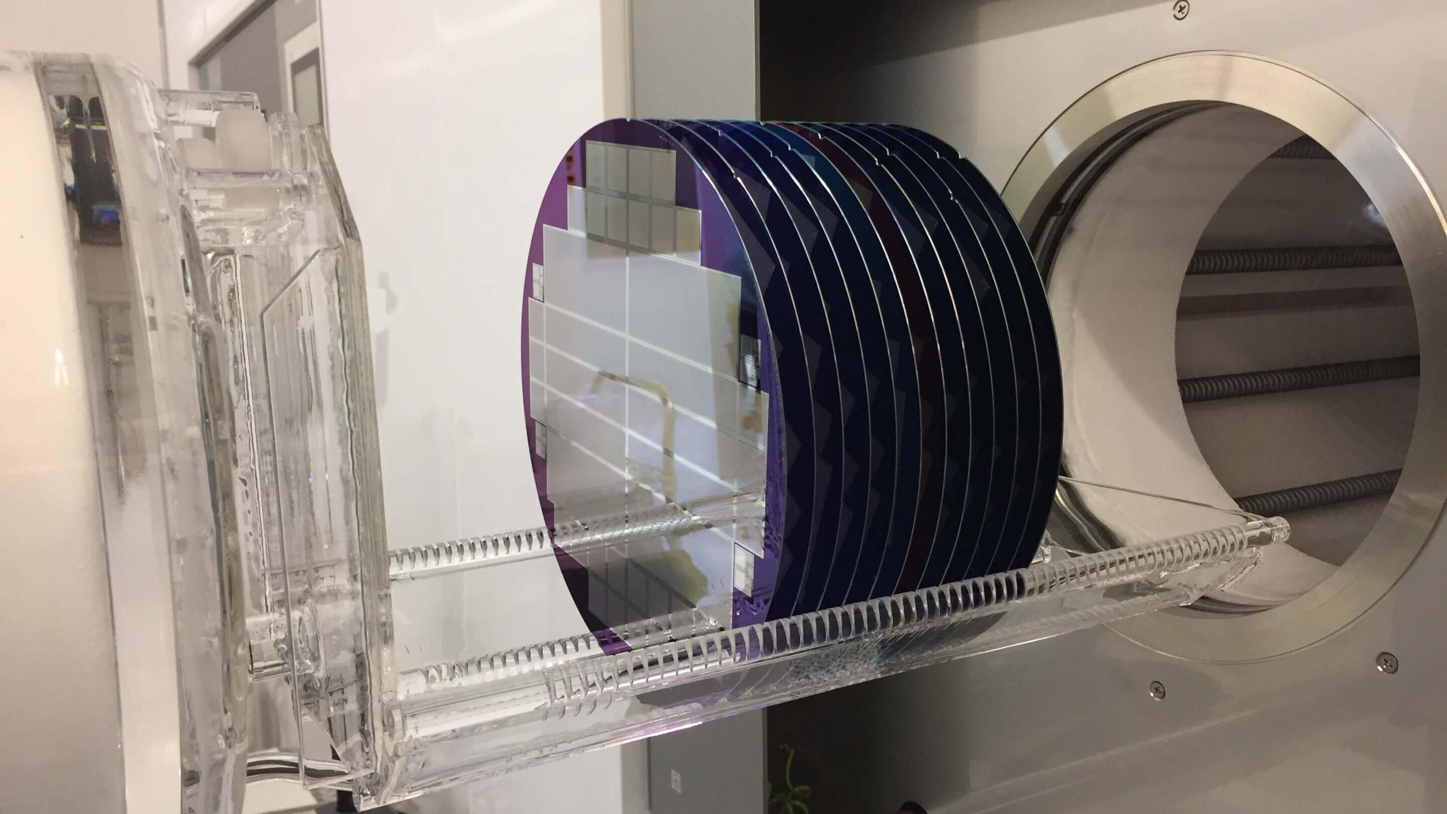
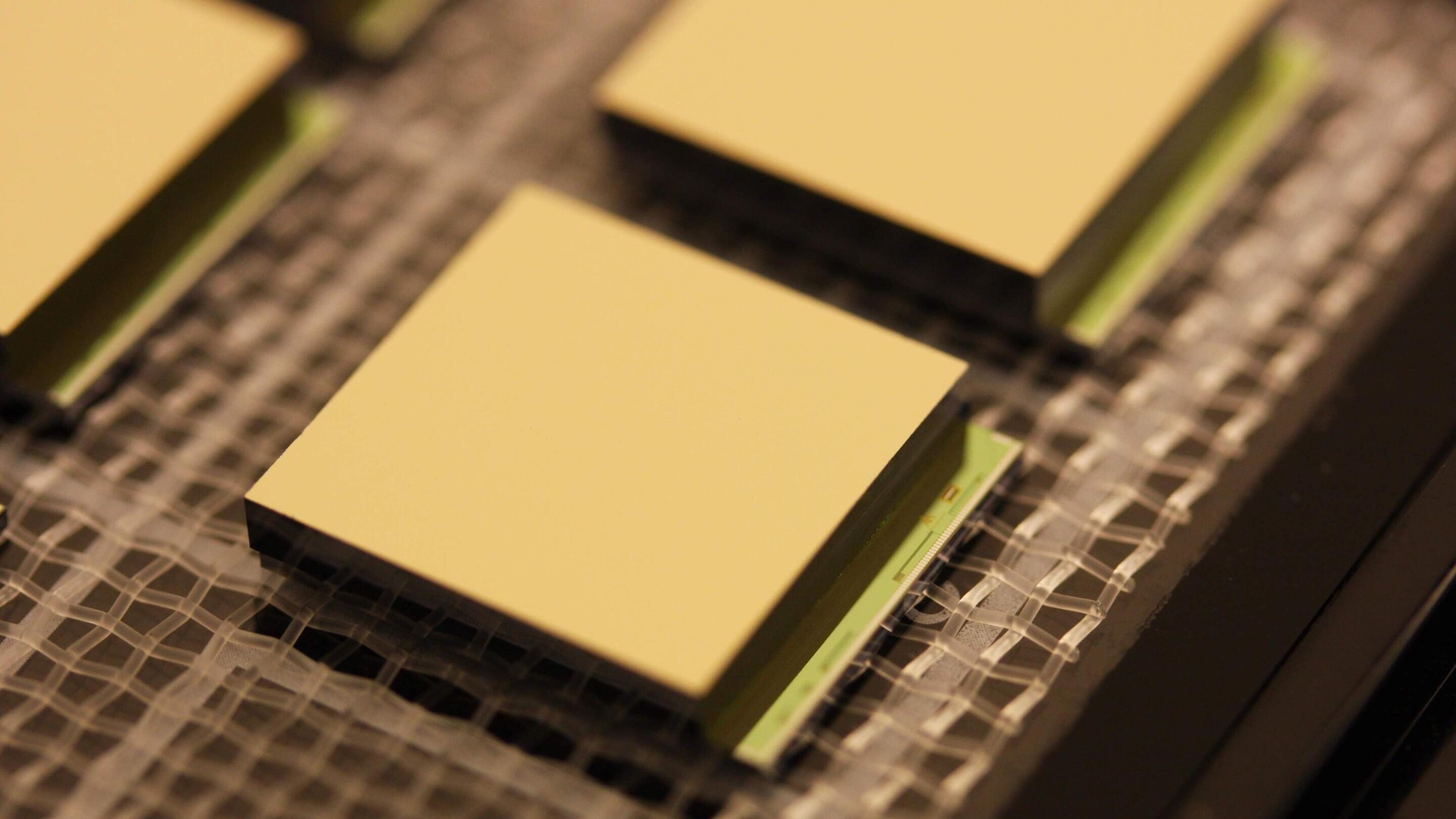
150 mm edgeless Si pixel sensor wafer manufacturing batch.
-
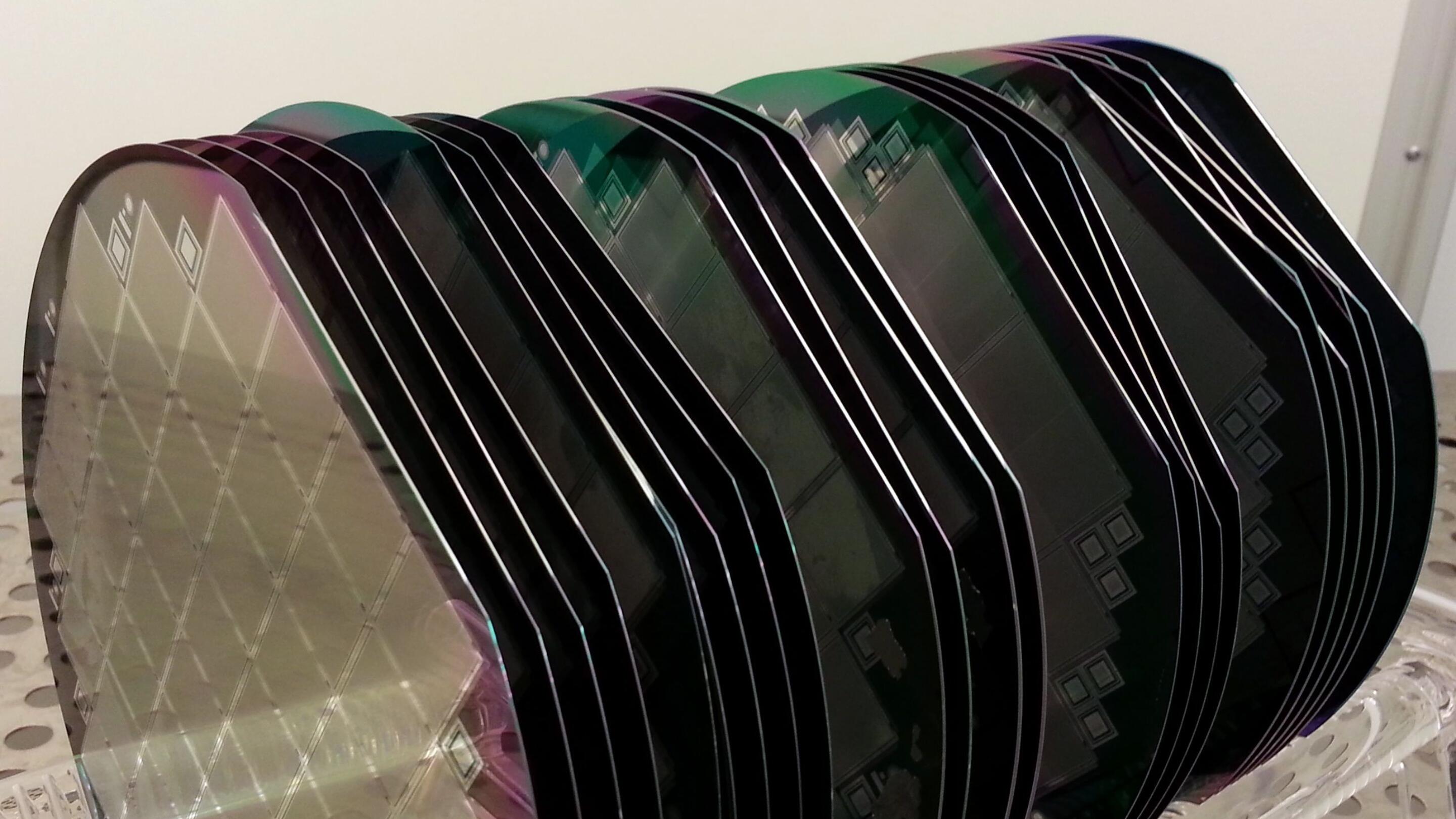
150 mm edgeless Si monolithic sensor wafer manufacturing batch.
Silicon-on-Insulator Sensor Manufacturing
Thin Silicon sensors, less than 300 um thickness, are manufactured using a silicon-on-insulator (SOI) technology maintain the mechanical integrity of the wafer through the sensor wafer process.
First the active sensor wafer in bonded on an oxidized handle wafer. Second the active sensor wafer is thinned to a desired thickness. After the standard planar manufacturing process steps and the UBM deposition, the handle wafer is removed and cathode metal layer is deposited.
As a final result thin sensor wafers from 10 to 200 um thickness are realized.
-
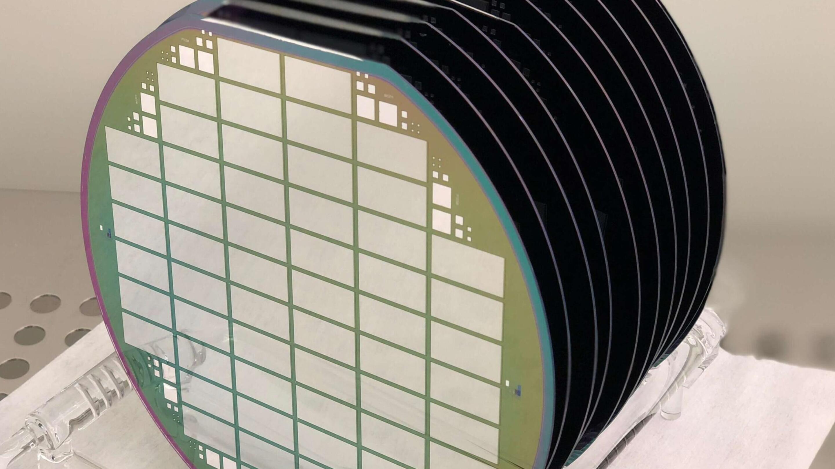
Batch of Atlas-Itk SOI sensor wafers.
-
Edge of an SOI sensor wafer where a 100 um thick active sensor wafer is bonded on a 380 um thick handle wafer.
-
Atlas-Itk 100 um thick sensor wafer after handle wafer removal.
Thin Entrance Window Sensor Manufacturing
Thin entrance window Si sensors are manufactured for low energy electron or X-ray imaging or spectroscopy.
In case of pixel sensor modules, the thin entrance window is made at the cathode electrode of the sensor. In case of diodes the thin entrance window is made on the anode side of the diode.
The thin entrance window is made by minimizing the thickness of the non-active layers, such as doping and metal contact on a silicon sensor. The non-active entrance window can be made as thin as few tens of nanometers.
-
Silicon is a lightweight semiconductor material that is widely used as an imaging sensor material. It is useful for low-energy radiation imaging and tracking. For X-ray imaging below 20 keV and electron imaging below 200 keV, Silicon has a good absorption efficiency.
GaAs Sensor Manufacturing
Advafab’s offering covers pixel, microstrip and diode sensors fabricated on 3” (75 mm) high resistivity GaAs wafers having a thickness of 500 um.
The GaAs wafer preparation for the spectral imaging sensors relies on in-house developed chromium compensation of the high resistive GaAs wafers. Using this method a uniform radiation response over the wafer can be obtained.
Due to high resistivity of GaAs the sensor is essentially edgeless and can be used to tile individual sensor side by side without an ineffective gap between the tiles.
-
Gallium Arsenide is a compound semiconductor material that is uniform and stable for imaging sensor material. It is useful for mid-energy radiation imaging and tracking. For X-ray imaging between 20-80 keV and electron imaging above 200 keV, Gallium Arsenide has a good absorption efficiency.
CdTe and CdZnTe Sensor Manufacturing
Advafab doesn’t have in-house capability to fabricate CdTe and CdZnTe sensors.
We work closely with the industrial leaders to fabricate the CdTe to CdZnTe sensors according to the customer’s specifications. The design of the sensor will be prepared by our experts and the sensors will be purchased from our relied partners.
Due to high resistivity of CdTe and CdZnTe the sensor is essentially edgeless and can be used to tile individual sensor side by side without an ineffective gap between the tiles.
-
Compound semiconductor sensors.
-
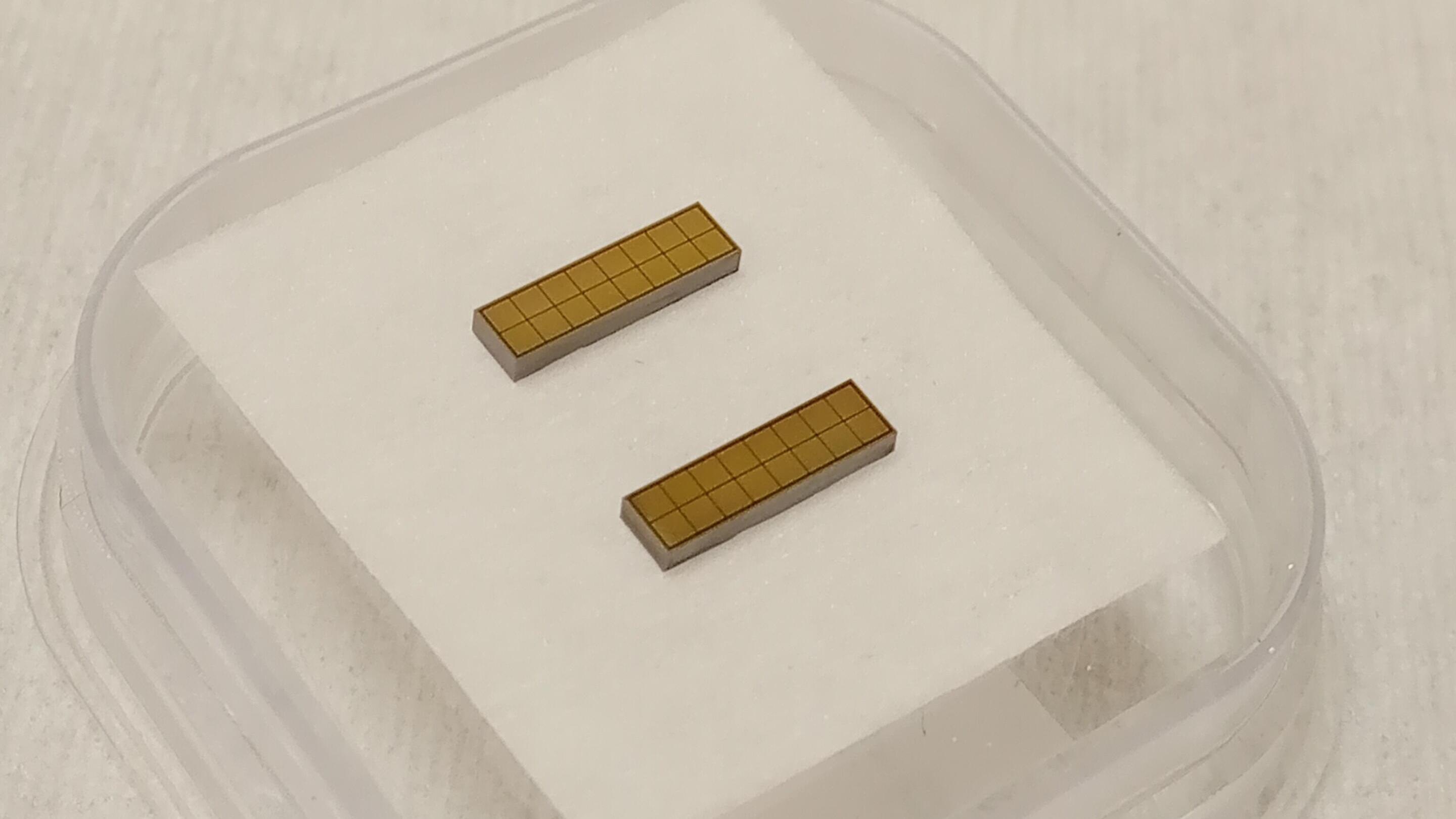
5 mm thick CdZnTe pixel sensor.
-

Different types of sourced compound semiconductor sensors.
-
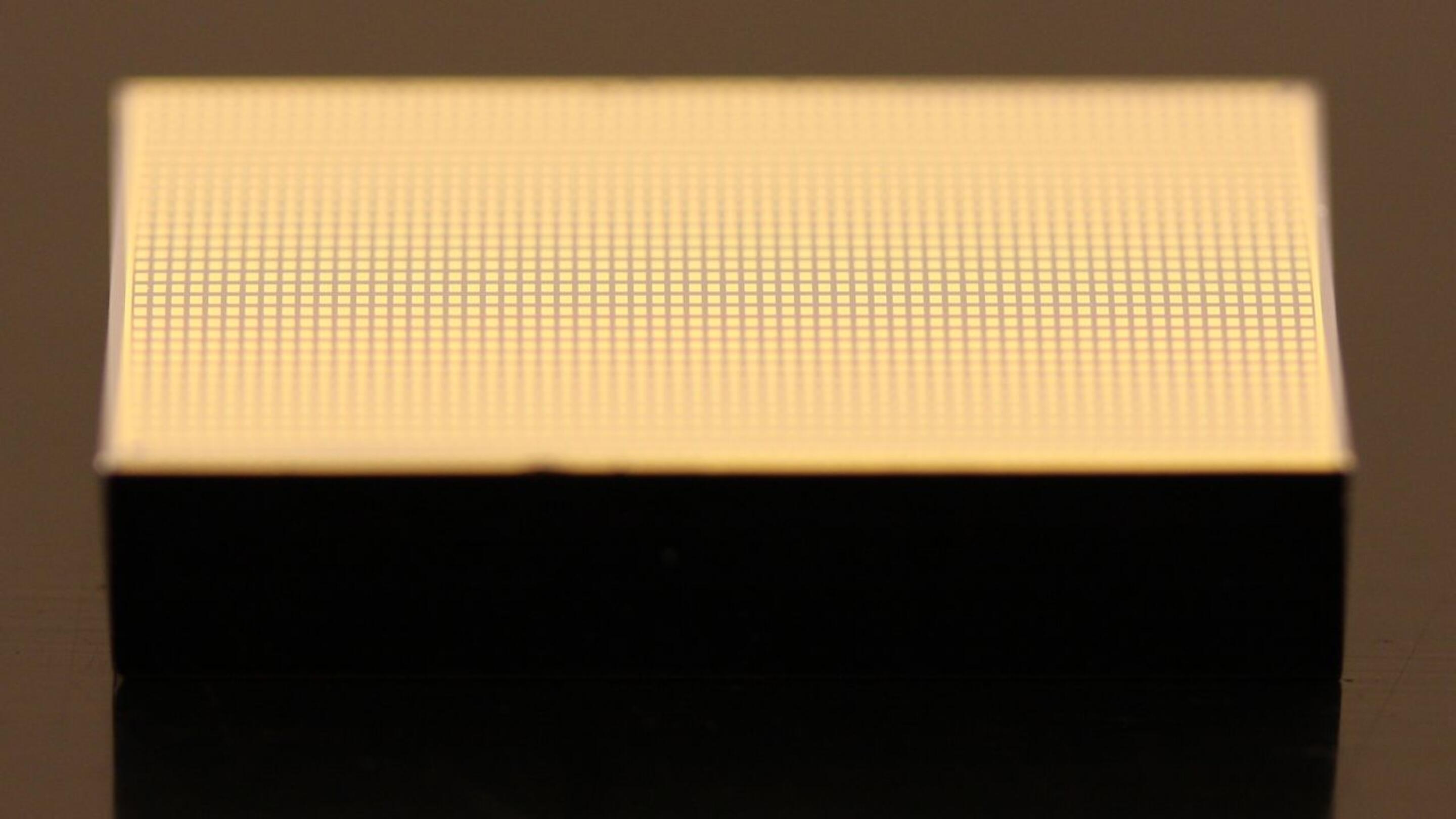
The compound semiconductors are challenging materials to be diced. Special dicing blades and dicing parameters are required for the materials.
-
Medipix ASIC flip chip bonded with 9 pcs of 4x4 mm2 CdTe pixel sensors side-by-side.
-
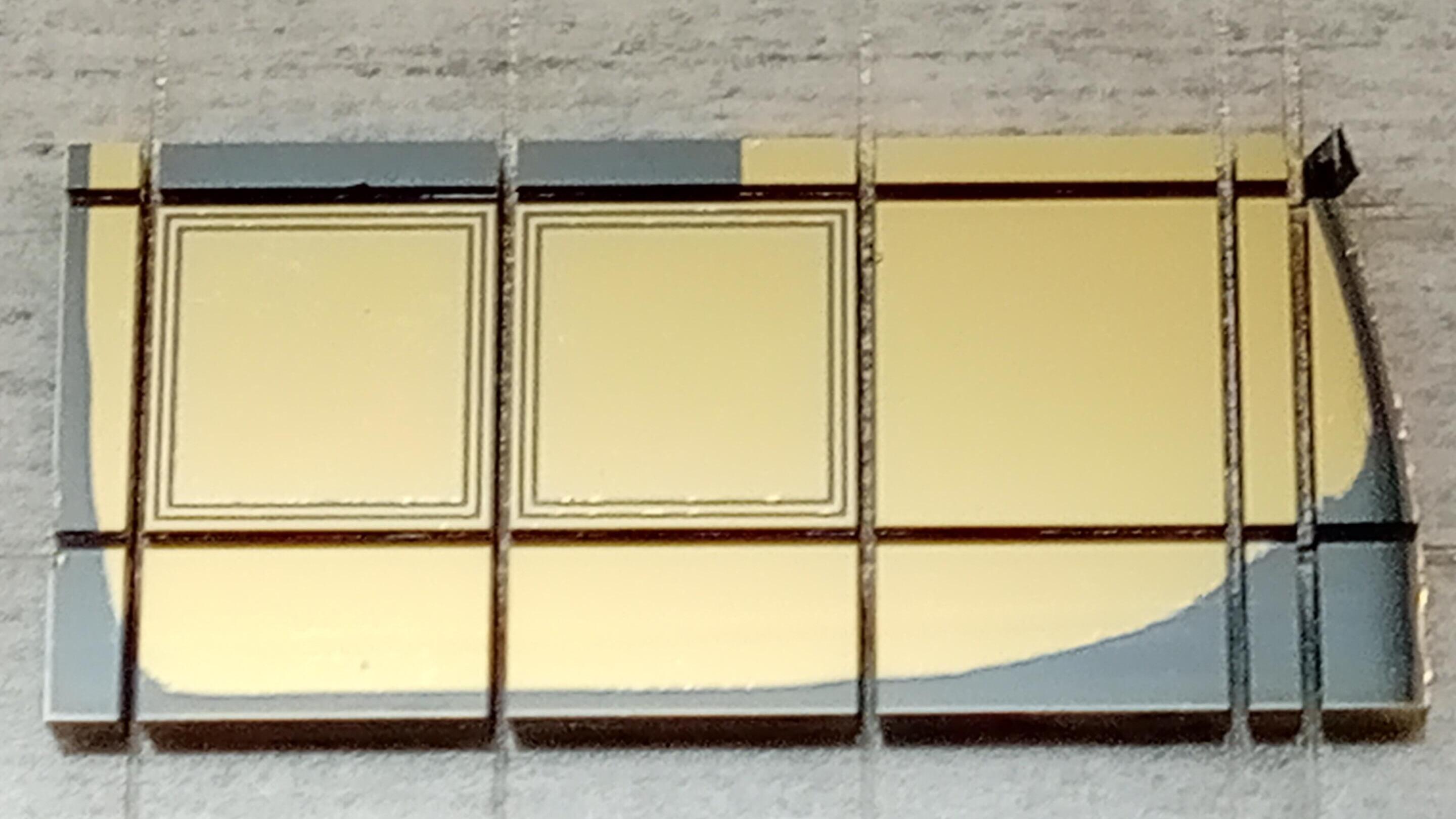
Flip chip bonded 2 mm thick CdTe sensor module.
-
Cadmium (Zinc) Telluride is a compound semiconductor material that is used as high-energy imaging sensor material. It is useful for high-energy radiation imaging and tracking. For X-ray imaging between 20-160 keV, Cadmium (Zinc) Telluride has a good absorption efficiency.
Enhance Your Devices with Our Next-Generation Semiconductors
Join the ranks of the most advanced technology users with our cutting-edge solutions
Our Services – We offer full service catalog from design to production
We offer a comprehensive suite of semiconductor services, expertly crafted to meet the demands of both small and large-scale productions as well as the most ambitious research & development projects.


