UBM – Solid Base for Soldering
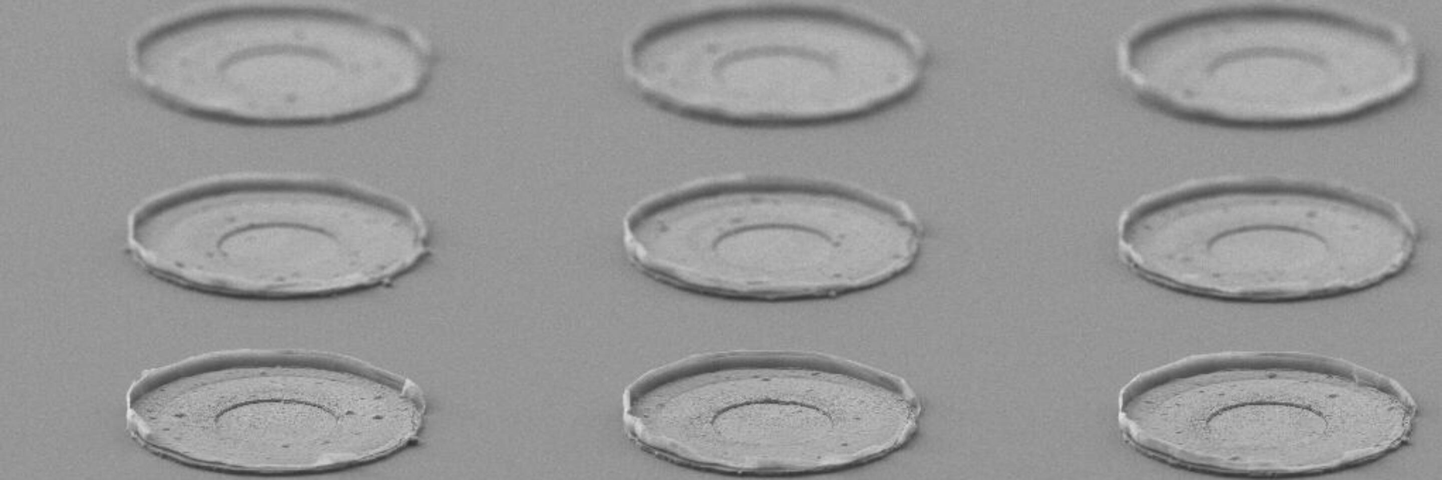
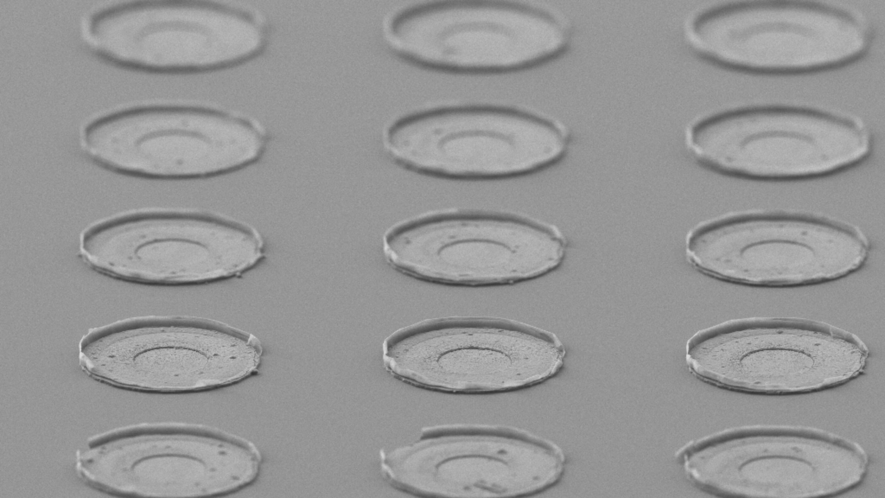
AdvaFab deliver thin film Under-Bump Metallization (UBM) pads on sensor wafers. The role of the UBM is to:
- Provide good and reliable surface finishing for soldering
- Act as diffusion barrier against the components of the solder alloy
- Provide good adhesion to the wafer.
The AdvaFab-deposited UBM pads are compatible with InSn, SnPb, AgSn and other typical solder alloys. The UBM pads have been designed to allow flip chip bonding of multiple dies on the chips and rework of some chips.
-
UBM process is available for AdvaFab fabricated Si sensor wafers (stand-alone and SOI wafers) and for third-party manufactured wafers. The process is available for thin stand-alone thin wafers with thickness starting from 100 um. The thin-wafer UBM process uses temporarily bonded carrier wafers to support the fragile wafers during the processing. The process is available for individual and mid-sized production volumes up to thousand wafers per year.
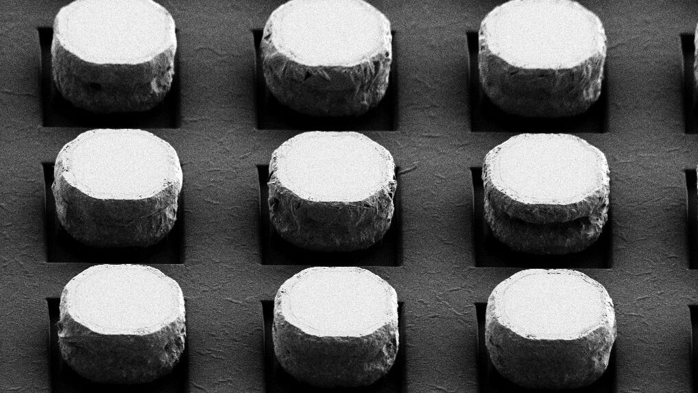
Besides the thin film UBM pads, electrodeposited UBM pas also be offered for 500 um thick or thicker sensor wafers. It is important that the wafer edge has been ground to increase the robustness of the wafers. The typical electrodeposited UBM pads are Ni/Au or Cu.

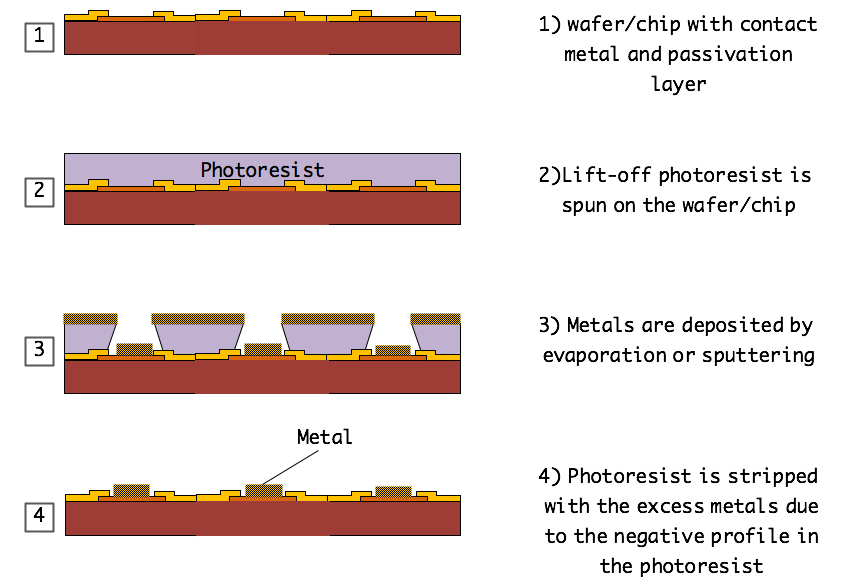
Simplified description of lift-off process
Enhance Your Devices with Our Next-Generation Semiconductors
Join the ranks of the most advanced technology users with our cutting-edge solutions
Our Services – We offer full service catalog from design to production
We offer a comprehensive suite of semiconductor services, expertly crafted to meet the demands of both small and large-scale productions as well as the most ambitious research & development projects.


