Wafer Bumping is the Corner Stone of Successful Flip Chip Bonding
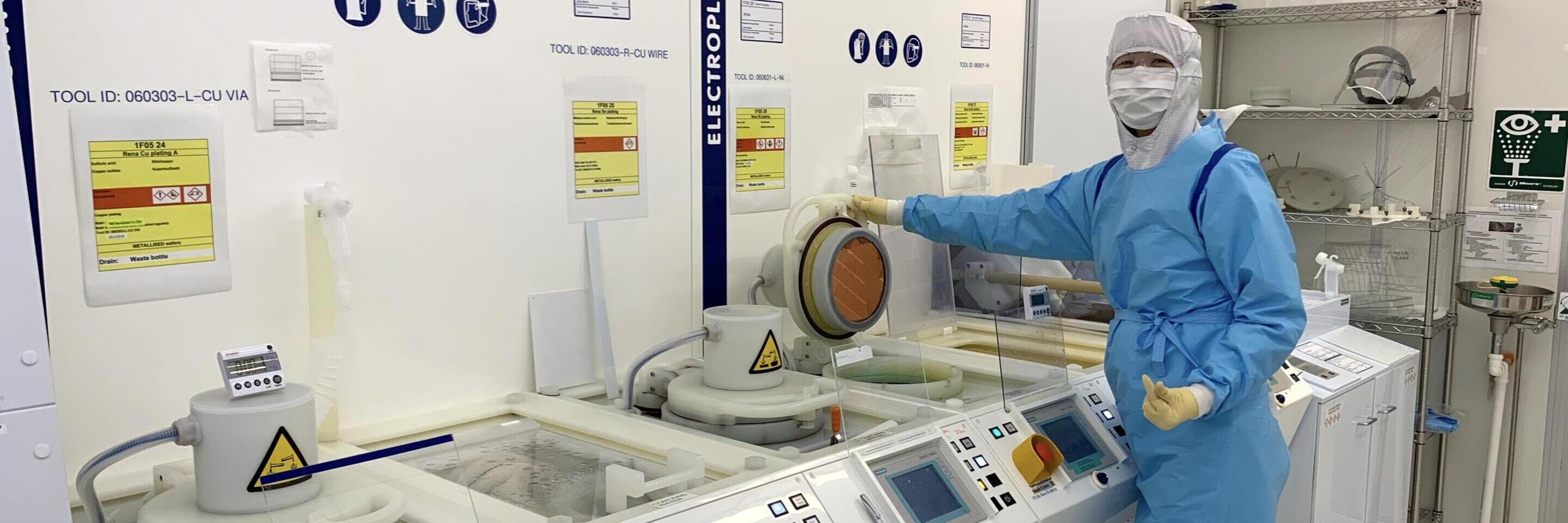
AdvaFab has been specialized in depositing of the low-melting point, indium-based solder bumps on wafers with large dies. Wafer bumping is done by electrodeposition for 150 mm to 200 mm wafers in-house. For larger wafers a coring service will be needed to 200 mm wafer or the work can be outsourced to the company’s production partners. During the wafer bumping process, the solder bumps are grown on each pixel on the ASIC wafer in parallel. The typical interconnect density is higher than 30,000 per cm2 which requires good size and compositional uniformity from the bumps to successfully hybridize the sensor module. The wafer bumping process is a corner stone for fabricating high-quality hybrid sensor modules. The service is available from single wafer prototyping projects to mid-size production of hundreds of wafers per year.
-
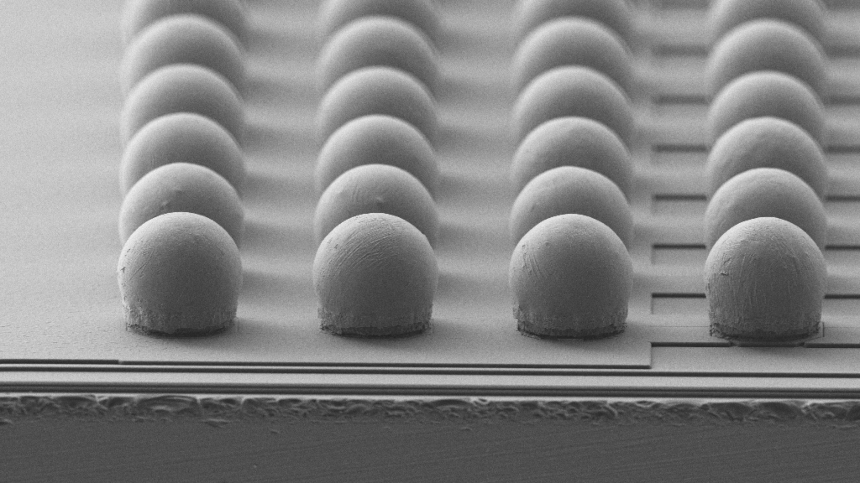
Wafer bumping can be done with 20 um – 200 um bump pitch. Solder bumps can be deposited as standard collapsible balls or ultra-fine pitch compatible pillar type of bumps. The minimum bump size is 13 um. Typical bumps have 18-25 um height after reflow.
The limiting factors above 200 um pitch is the minimum required plating area required on the wafer to have predictable electrodeposition rates. Dummy bumps are added on the wafers outside the dies of interest to increase the plating area.
Maximum height of the bumps is limited by the thin film lithography. The electroplating should take place at the resist openings at each pixel to control the current density and electrodeposition rate. This is important to aim for certain solder composition by depositing stack of different metals such as indium and tin.
-
Lead-free InSn solder bumps are a great choice for flip chip bonding of compound semiconductor sensors. The eutectic melting point is very low (118C) and the alloy is very soft and ductile. The In-based bumps suit very well to low temperature applications and for sensors modules where it is beneficial to flip chip bond or rework modules at low temperatures. Low solderering temperature is particularly useful when flip chip bonding Cd(Zn)Te or GaAs sensors where there will be thermo-mechanical stresses because of different coefficients of thermal expansions.
Lead-free AgSn solder is the industry standard and it suits well for various Si modules.
For special exemptions allowed by the RoHs directive SnPb solder will be available until the end of 2023. Eutectic SnPb (63:37) has superior wetting characteristics and it is more UBM-friendly than AgSn and AgCuSn lead-free solder alloys.
AdvaFab’s solder bump structures are designed such a way that the ASICs can be reworked from the sensors in case of poor flip chip bonding quality or electrically malfunctioning.
-
Cu (copper) pillars are solder interconnects that have a tall copper foot and solder ball on top. The profile of the Cu pillar bumps is way slimmer than that of the traditional collapsible bumps with low-profile UBM pads, and they suit particularly well for flip chip bonding of chips with ultra-fine pitch (< 50 um). The small solder caps on top of the pillars reduces the risk of having solder bridges between the adjacent interconnects during flip chip bonding. Moreover, the pillars can provide higher current carrying capacity and stand-off height between the bonded chips.
-

Steps in wafer bumping by electrodeposition: 1) wafer with close-up to one pixel, 2) metallisation of the wafer with adhesion and conductive seed layer, 3) photolithography, 4) electrodeposition of the UBM, 5) electrodeposition of the elements in the solder alloy, 6) removal of the photoresist, 7) etching of the seed layer and 8) adhesion layer, 9) reflow
-
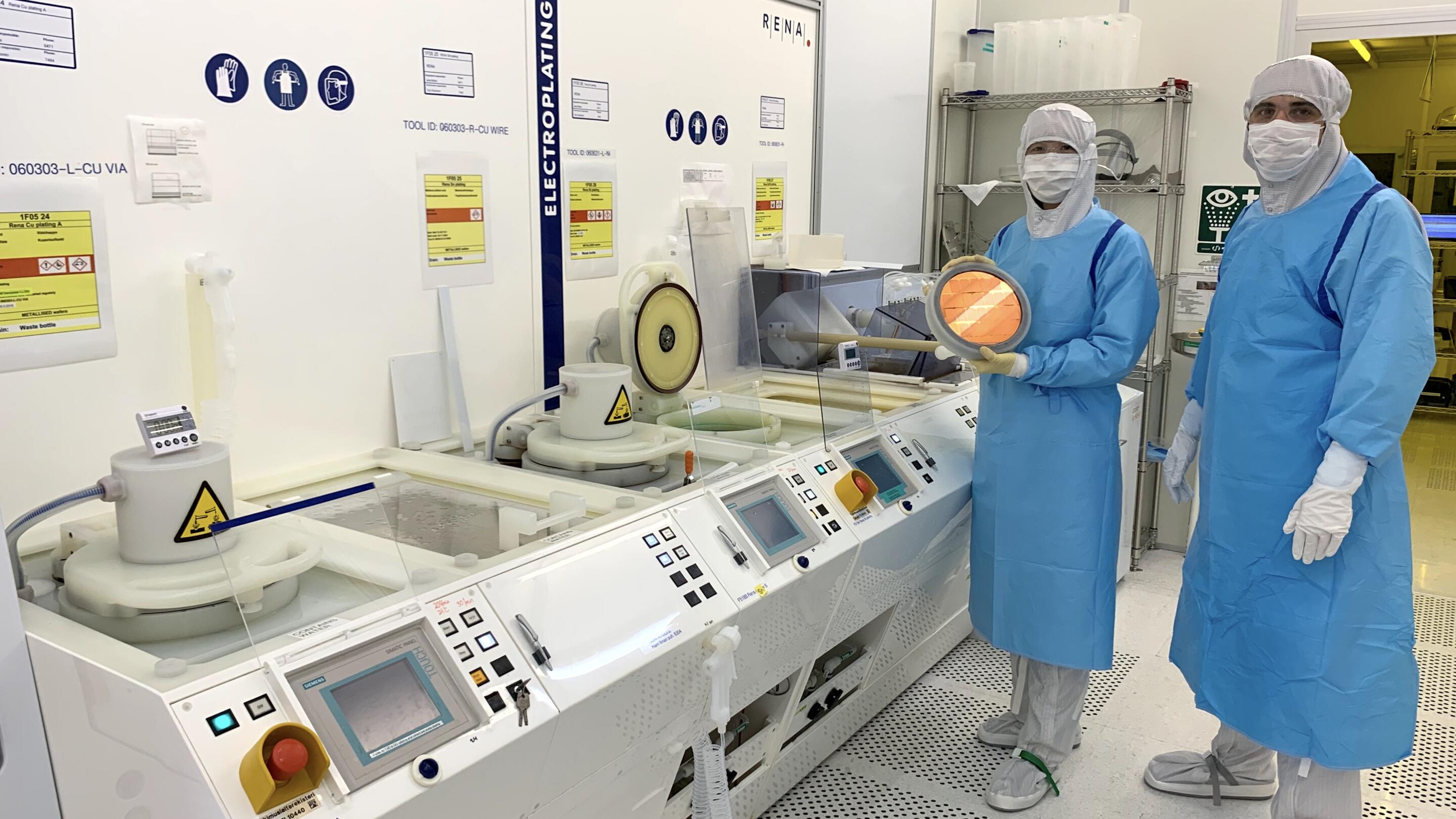
In electroplating, the wafers our mounted in chucks which make an electrical contact to the seed layer (typically Cu) on the wafer to enable galvanic deposition from the electrolyte solutions.
-
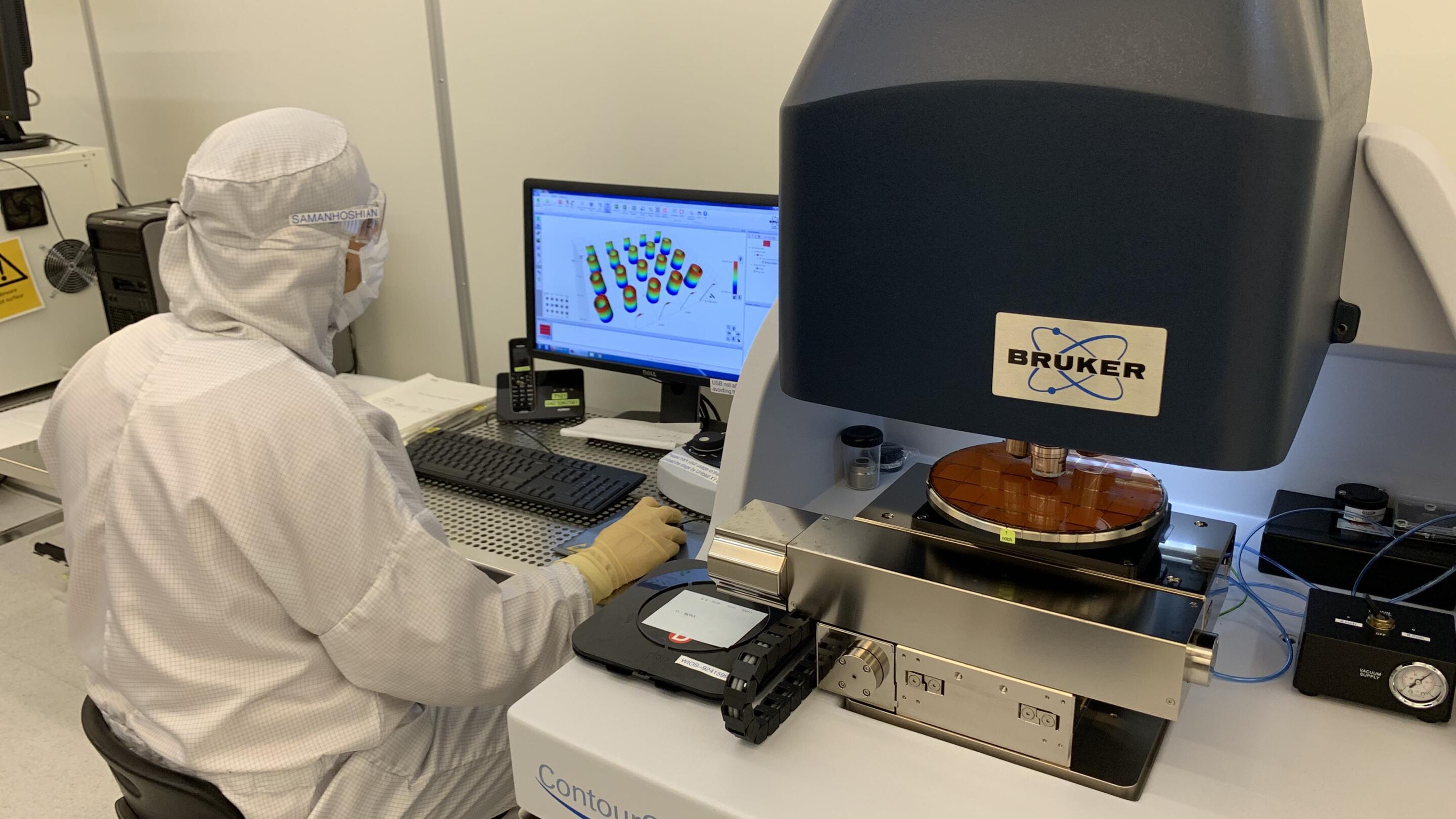
The height of the electroplated metals will be measured on wafer-level to be sure that the target thickness and uniformity have been met.
-
Enhance Your Devices with Our Next-Generation Semiconductors
Join the ranks of the most advanced technology users with our cutting-edge solutions
Our Services – We offer full service catalog from design to production
We offer a comprehensive suite of semiconductor services, expertly crafted to meet the demands of both small and large-scale productions as well as the most ambitious research & development projects.


