High-Performance Si PIN Diodes
Silicon PIN diodes are used in radiation detectors to measure the intensity or spectral response of ionizing radiation. PIN diodes have a high sensitivity to various radiation types, such as X-ray, α- and β-particles, and can provide accurate readings with fast response times.
Advafab manufactures and supplies customer-specific Si PIN diodes. The design is defined together with the customer and our experts to reach the best possible performance for the manufactured diodes.Typically thin entrance window is implemented on the anode side of the diode to enhance the sensitivity of the diode for low energy radiation.
The performance of the Si PIN diode is typically assessed by leakage current, capacitance and energy resolution. Advafab is able to reach very low leakage current below 1 nA/cm2 with its fine-tuned process and usage of the best Silicon wafer starting material.
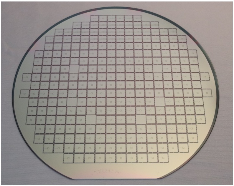
Low leakage current Si PIN diode wafer manufactured at Advafab.
Quality of the Si PIN Diodes
The Si PIN diode wafers are electrically characterized on the wafer level to verify the conformity of delivered products.
The wafer level measurement is done using an automated wafer probe station and a high-precision parameter analyzer. The measurement results are inserted into a database and delivered to the customer together with the diced wafers. The electrical characterization report clearly visualizes the conforming dies and it can be directly used as input for a pick-and-place machine for die sorting in the assembly line.
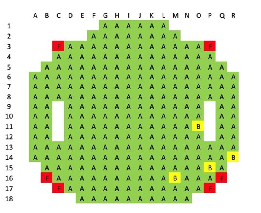
Example of electrically characterized high yield Si PIN diode wafer.
High-Performance Si 1D Sensors
Similarly to Si PIN diodes, Advafab manufactures customer-specific 1D sensors, or segmented diodes, with low leakage current and inter-strip capacitance.
The Si 1D sensors can be manufactured with a variety of thicknesses from a few micrometers to a millimeter. Typically the Si 1D sensors manufactured are DC-coupled. Advafab has also technologies available for AC-coupling of the strips.

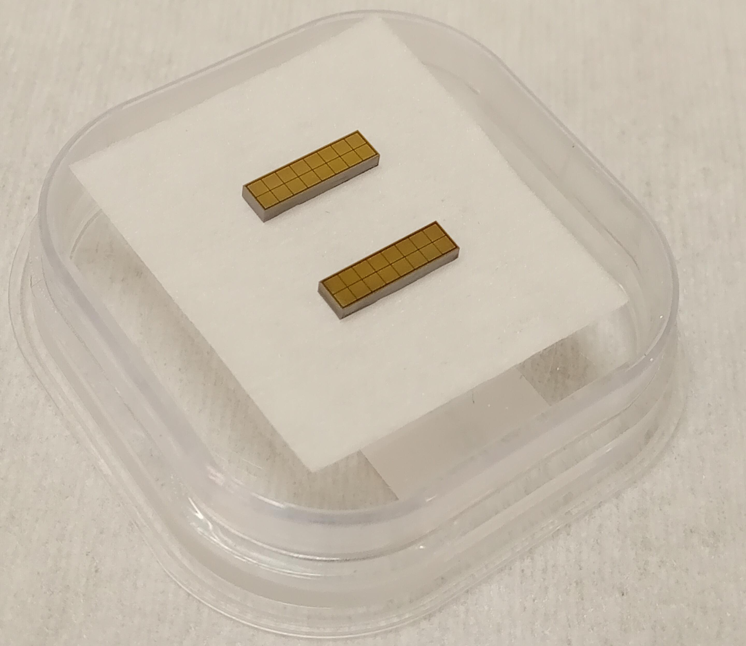
Image of strip, pixel and pad sensors.
Compound Semiconductor Diodes and 1D Sensors
Advafab is internally able to manufacture GaAs compound semiconductor diodes and 1D sensors. For the Cd(Zn)Te diodes and 1D sensors, Advafab works closely with its trusted partners.
The GaAs diodes and 1D sensors can be ordered from custom design to delivery of the electrically and spectroscopically measured sensor. In case of Cd(Zn)Te, Advafab makes the customer specific design and outsources the manufacturing of the diodes and 1D sensors and makes sure the the desired electrical and spectral specifications are met in the delivery.
Compound semiconductor sensors.
Assembling of Manufactured Components
Advafab works closely with its trusted partners to offer small to large-scale PCB-level assembling of the Si PIN and 1D sensors.
Advafab’s customers are able to outsource the design and manufacturing of the PCBs together with mounting and wire bonding of Advafab-manufactured conforming products on the PCB.
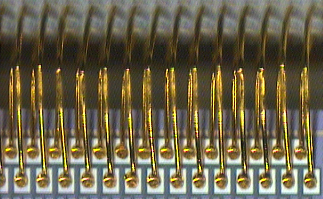
Wire bonding of 1D sensors.
Semiconductor Materials for Diodes and 1D Sensors
Each of these materials has its own unique properties and advantages, which make them suitable for different applications.
Enhance Your Devices with Our Next-Generation Semiconductors
Join the ranks of the most advanced technology users with our cutting-edge solutions
Our Services – We offer full service catalog from design to production
We offer a comprehensive suite of semiconductor services, expertly crafted to meet the demands of both small and large-scale productions as well as the most ambitious research & development projects.


