Usage of Silicon Sensors
Silicon sensors are commonly used in a broad range of energy levels, from low-energy applications to high-energy applications.
The suitability of silicon sensors for specific energy ranges and radiation types depends on the selected Si material, design, process and thickness.
Here are some typical energy ranges and applications where silicon sensors are employed:
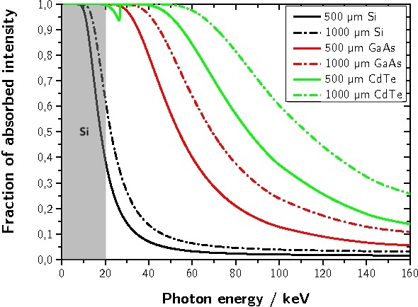
- Low-Energy X-rays: Silicon sensors can effectively detect and measure X-rays in the low-energy range up to 20 keV. This includes applications such as X-ray imaging, X-ray spectroscopy, and low-energy gamma-ray detection

X-ray absorption in Si sensor and its usable energy range. Source publication
- Low-Energy electrons: Silicon sensors can effectively detect and measure electrons in energy range from 5 keV to 200 keV. This includes applications such as Transmission Electron Microscopy (TEM), Scanning Electron Microscopy (SEM), and Electron Energy Loss Spectroscopy (EELS)
- Medium Energy particles: Silicon sensors are also utilized in the medium-energy range for the detection of accelerated particles, typically in the megaelectronvolt (MeV) range. The Si sensor are used for radiation detection and measurement in applications such as radiation therapy, nuclear medicine, and environmental monitoring for radioactive materials.
- High Energy particles: Silicon sensors are employed in high-energy physics experiments, such as particle colliders and cosmic ray experiments, where particles with energies ranging from billions of electronvolts (GeV) to trillions of electronvolts (TeV) are detected. These sensors enable the tracking and measurement of high-energy particles produced in these experiments.
Silicon Semiconductor Material
Silicon is one of the most useful elements to mankind because vast majority of semiconductor devices are made of it.
Silicon is the best semiconductor material for various devices, because it is available in larger wafers; the material is widely commercially available in many different grades; its price is low; it has very good uniformity etc. In this page the journey of silicon is described from sand to wafers in a simplified manner.
-
Silicon is the eighth most common element in the universe by mass, but very rarely occurs as the pure element in the Earth’s crust. More than 90% of the Earth’s crust is composed of silicate minerals, making silicon the second most abundant element in the Earth’s crust (about 28% by mass), after oxygen. The base ingredient of any semiconductor-grade silicon is extracted from desert sand. If someone states that world will run out of silicon, the limiting factor won’t be the amount of available raw material.
Silicon material is found abundantly in the earth’s crust in compounds that consists of around 25% to 50% silicon dioxide. Most elemental silicon produced remains as a ferrosilicon alloy, and only approximately 20% is refined to metallurgical grade purity. About 15% of the world production of metallurgical grade silicon is further refined to semiconductor purity. This typically is the “nine-9” or 99.9999999% purity, nearly defect-free single crystalline material. It’s not easy to find a material with better purity than that of Si.

Sand comprises mostly of silicon oxide -
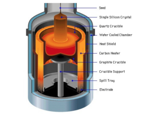
Semiconductor-grade Silicon is grown as ingots using different techniques. The growth technique has a major contribution to the number of impurities in Si. The vast majority of Si used for semiconductor devices is grown using Czochralski (CZ) method. The Si used by the CMOS foundries is typically CZ Si and it is available in up to 450 mm wafers. In the CZ method, a fused silica crucible in a furnace is filled with electronic-grade polysilicon. The desired dopant atoms are added either in the form of doped Si or in elemental form. A small single crystal seed piece of known crystal orientation is dipped into molten Si and pulled out of the melt. During the crystal pulling process, the grown Si ingot and the crucible with molten Si are rotated in opposite directions. In the Czochralski growth, the fused silica crucible dissolves slowly in the molten liquid and contributes to the number of impurities. The most common impurities are carbon, oxygen, aluminum and boron and they’ll end up in the grown Si ingot in some extent.

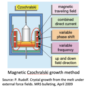
Magnetic Czochralski growth method
Source: Lecture on silicon floatzone czochralskiThe detector grade Si has typically very high purity and is typically grown using Float Zone (FZ) or Magnetic CZochralski (MCZ) methods and the size of the wafers is limited to 200 mm size. Most of the Si used for pixel detectors and power electronics is using FZ silicon, because of its high purity and resistivity. The MCZ silicon differs from the typical CZ, because it has fewer impurities thanks to the magnetic fields that are applied during the crystal growth. The magnetic field reacts with the molten Si and it, and it has an impact on the concentration and amount of the impurities in the grown Si crystal.

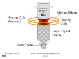
An illustration of MCZ crystal growth method with traveling magnetic fields. The float zone (FZ) Si is very clean and its resistivity can be up to 30k-Ohm-cm. The major advantage is the crucible-less growth that prevents contamination of the silicon from the vessel itself. In FZ growth process an ultra-pure rod of electronic-grade polysilicon rod with a seed crystal at the end will be scanned by the heating coils. The process is carried out in an evacuated process chamber or under inert pure gas. The moving heating element will create a localized molten zone in the Si leading to high-purity single-crystal silicon.

Float zone Si is grown from ultra-high purity polysilicon rod. The local heating zone minimizes the molten volume of Si and leads to fewer impurities and other imperfections compared to growth methods pulling the crystals from molten Si. -
After the growth of the ingot, the ingot will be sliced to wafers with a wire saw. The wafers will be further ground to close to the target thickness and polished. The purpose of the grinding and polishing steps is to have a smooth Si surface. The polishing step will remove damage layer on the Si surface left by the grinding process. After polishing the surface of the wafer is practically defect free and the wafers are mechanically robust. The wafers can be single side or double side polished.
-
Sensor grade silicon wafer processing requires cleanliness from the process line. The high resistivity Si wafers are sensitive to any organic or inorganic contamination. Any organic or metallic impurities that cannot be cleaned from the Si wafers before the high temperature annealing or oxidation (> 1000C) steps will diffuse to the lattice of Si and ruin the high resistivity (i.e., purity of material) and leads to degradation of the electrical characteristics of the devices. Even small traces of impurities will contaminate the Si wafers during annealing steps because of increased diffusion rate. The impurities can be seen as reduced lifetime of the charge carriers and as increased leakage current in silicon detectors. Metallic impurities like copper or gold ruin the semiconductor properties of Si. The so-called IC clean processes only allow very limited number of metals to be processed on them (I.e., Al, Mo, Ti etc.)
Learn more about other Semiconductor Materials
Enhance Your Devices with Our Next-Generation Semiconductors
Join the ranks of the most advanced technology users with our cutting-edge solutions

