-
Sensor Manufacturing
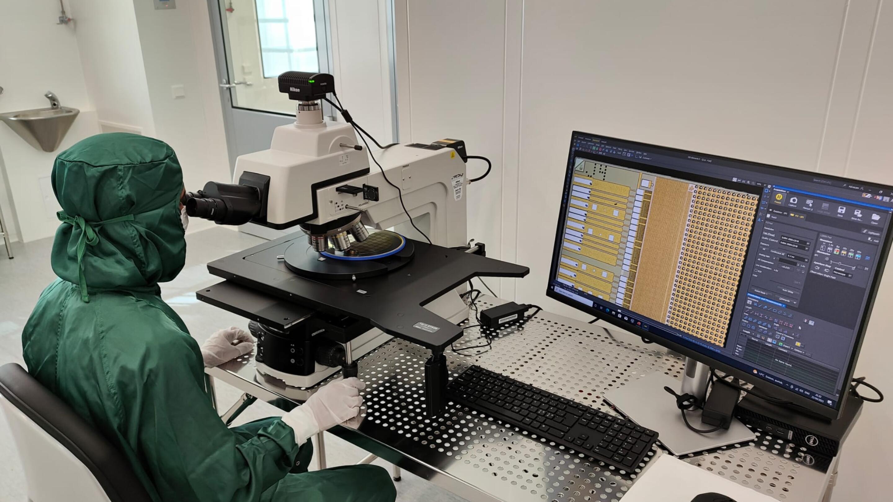
Advafab is used to working with wide variety of different customer specifications. Company’s sensor manufacturing process is flexible and always tailored to meet even the most demanding production and development requirements.
-
Under-Bump Metallization
Advafab has developed an optimal under-bump metallisation structure for the flip chip bonding of the semiconductor dies, to gain the best possible wetting for solder alloys.
-
Wafer Solder Bumping
Advafab uses electrodeposition in growing the solder bumps on the semiconductor wafers. The good size uniformity of the bumps is perhaps the biggest contributor to success rate of flip chip bonding for ultra-fine pitch sensor modules.
-
Flip Chip Bonding
Advafab uses solder bump-based flip chip bonding technology that is very precise, reliable and provides great repeatable results. Our deep understanding connected with tight process control ensures high quality pixel sensor modules.
-
Dicing
Advafab’s experts select the optimal dicing technique based on the wafer material and customers requirements, delivering high-quality and precise cut.
-
Electrical Measurement
Advafab uses electrical measurements to ensure our customers receive high-quality products, that meet their specifications and perform optimally in their applications.
-
Mask Design
Advafab's mask design services utilize state-of-the-art techniques to produce precise, accurate, and high-quality photolithography masks for semiconductor manufacturing.
-
X-ray probing
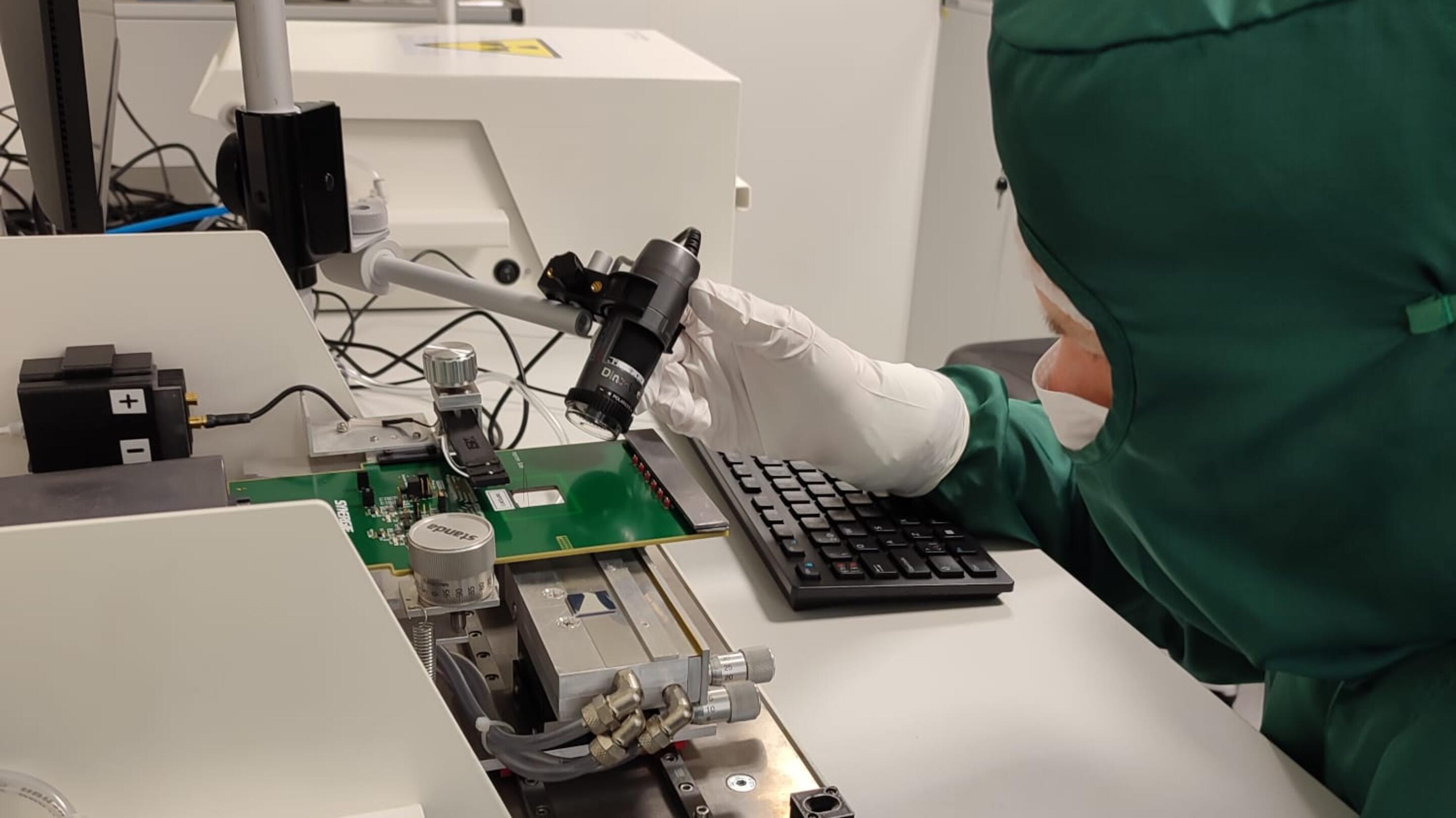
Advafab uses X-ray probing technique to ensure the quality of the flip-chip bonded modules. This non-destructive method guarantees the interconnection quality and performance of the sensor.
-
Wire Bonding
Advafab offers guaranteed high-quality mounting and wire bonding of its products together with its trusted partner.
Ensuring quality and reliability in our semiconductor production
Quality assurance is a vital step in the semiconductor production process to guarantee that the final product meets industry standards and customer expectations. We hold the ISO9000:2015 quality certificate and have full traceability for our manufacturing and business processes. The secret sauce is our experienced team and thorough characterisation methods of the fabricated components.
Ensuring Excellence With Turnkey Solutions
AdvaFab is supplying hybridized pixels sensor modules to various companies and academic institutions. We provide a full suite of services including sensor manufacturing, UBM deposition, wafer bumping and flip chip bonding. We provide turnkey solutions to our customers supplying the sensor modules with agreed specifications and outsourcing the board-level assembly steps. Being liable for the whole value chain AdvaFab simplifies its clients’ logistics chain, improves the fabrication yield, and reduces fabrication costs.
-
We believe in starting our quality assurance process with a thorough evaluation of the design and specifications. This helps us identify any potential risks or areas for improvement and ensure that our production meets industry standards and customer expectations.
-
In our production process, we implement strict monitoring procedures to ensure that all industry standards are met. Additionally, regular inspections and tests are conducted to detect and prevent defects in our products. If any issues are found, we have a system in place to quickly resolve them and prevent them from happening again in the future.
-
We understand the importance of using high-quality materials in our production. That’s why we have established relationships with our suppliers to ensure that the materials used meet our standards. Our team regularly reviews the performance of our suppliers and implements improvements to our processes where necessary. By managing our suppliers effectively, we can guarantee the quality of the materials used in our production and the reliability of our final products.
Enhance Your Devices with Our Next-Generation Semiconductors
Join the ranks of the most advanced technology users with our cutting-edge solutions


